- 您現(xiàn)在的位置:買賣IC網(wǎng) > PDF目錄377825 > M40Z300WMH6TR (意法半導(dǎo)體) 5V or 3V NVRAM Supervisor for Up to 8 LPSRAMs PDF資料下載
參數(shù)資料
| 型號(hào): | M40Z300WMH6TR |
| 廠商: | 意法半導(dǎo)體 |
| 英文描述: | 5V or 3V NVRAM Supervisor for Up to 8 LPSRAMs |
| 中文描述: | 5V或3V NVRAM中監(jiān)多達(dá)8個(gè)LPSRAMs |
| 文件頁(yè)數(shù): | 8/21頁(yè) |
| 文件大?。?/td> | 132K |
| 代理商: | M40Z300WMH6TR |
第1頁(yè)第2頁(yè)第3頁(yè)第4頁(yè)第5頁(yè)第6頁(yè)第7頁(yè)當(dāng)前第8頁(yè)第9頁(yè)第10頁(yè)第11頁(yè)第12頁(yè)第13頁(yè)第14頁(yè)第15頁(yè)第16頁(yè)第17頁(yè)第18頁(yè)第19頁(yè)第20頁(yè)第21頁(yè)
M40Z300, M40Z300W
8/21
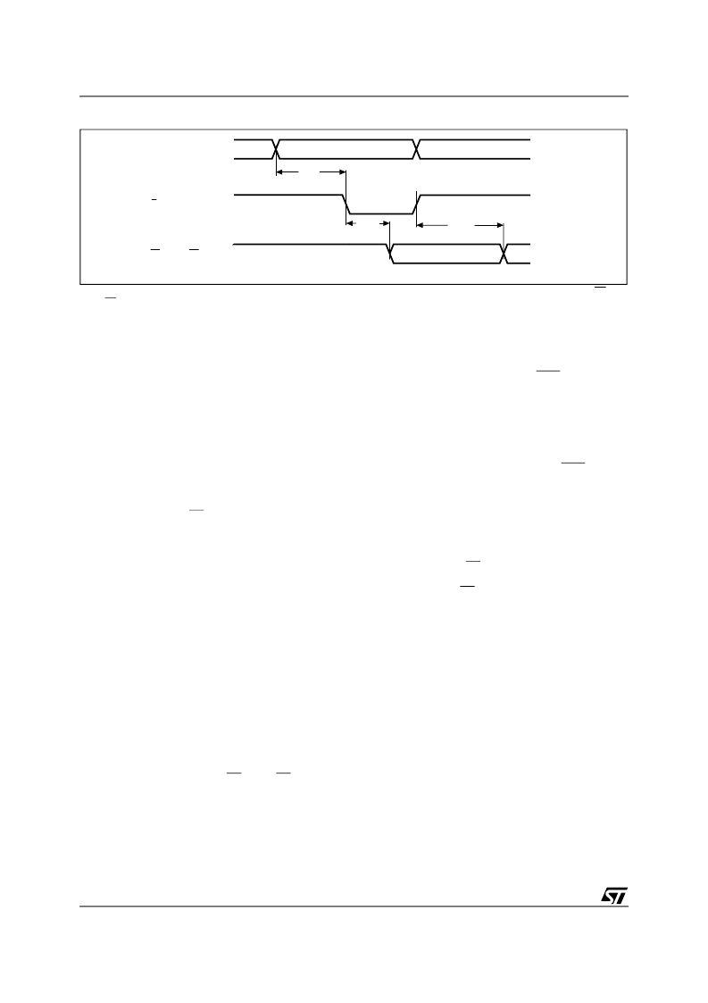
Figure 8. Address-Decode Time
Note: During system design, compliance with the SRAM timing parameters must comprehend the propagation delay between E1
CON
-
E4
CON
.
Data Retention Lifetime Calculation
Most low power SRAMs on the market today can
be used with the M40Z300/W NVRAM SUPERVI-
SOR. There are, however some criteria which
should be used in making the final choice of which
SRAM to use. The SRAM must be designed in a
way where the chip enable input disables all other
inputs to the SRAM. This allows inputs to the
M40Z300/W and SRAMs to be “Don't Care” once
V
CC
falls below V
PFD
(min). The SRAM should also
guarantee data retention down to V
CC
= 2.0V. The
chip enable access time must be sufficient to meet
the system needs with the chip enable propaga-
tion delays included. If the SRAM includes a sec-
ond chip enable pin (E2), this pin should be tied to
V
OUT
.
If data retention lifetime is a critical parameter for
the system, it is important to review the data reten-
tion current specifications for the particular
SRAMs being evaluated. Most SRAMs specify a
data retention current at 3.0V. Manufacturers gen-
erally specify a typical condition for room temper-
ature along with a worst case condition (generally
at elevated temperatures). The system level re-
quirements will determine the choice of which val-
ue to use.
The data retention current value of the SRAMs can
then be added to the I
BAT
value of the M40Z300/
W to determine the total current requirements for
data retention. The available battery capacity for
the SNAPHAT
of your choice can then be divided
by this current to determine the amount of data re-
tention available (see
Table 13., page 19
).
CAUTION:
Take care to avoid inadvertent dis-
charge through V
OUT
and E1
CON
- E4
CON
after
battery has been attached.
For a further more detailed review of lifetime calcu-
lations, please see Application Note AN1012.
Power-on Reset Output
All microprocessors have a reset input which forc-
es them to a known state when starting. The
M40Z300/W has a reset output (RST) pin which is
guaranteed to be low within t
WPT
of V
PFD
(see
7
).
This signal is an open drain configuration. An ap-
propriate pull-up resistor should be chosen to con-
trol the rise time. This signal will be valid for all
voltage conditions, even when V
CC
equals V
SS
.
Once V
CC
exceeds the power failure detect volt-
age V
PFD
, an internal timer keeps RST low for
t
REC
to allow the power supply to stabilize.
Battery Low Pin
The M40Z300/W automatically performs battery
voltage monitoring upon power-up, and at factory-
programmed time intervals of at least 24 hours.
The Battery Low (BL) pin will be asserted if the
battery voltage is found to be less than approxi-
mately 2.5V. The BL pin will remain asserted until
completion of battery replacement and subse-
quent battery low monitoring tests, either during
the next power-up sequence or the next scheduled
24-hour interval.
If a battery low is generated during a power-up se-
quence, this indicates that the battery is below
2.5V and may not be able to maintain data integrity
in the SRAM. Data should be considered suspect,
and verified as correct. A fresh battery should be
installed.
If a battery low indication is generated during the
24-hour interval check, this indicates that the bat-
tery is near end of life. However, data is not com-
promised due to the fact that a nominal V
CC
is
supplied. In order to insure data integrity during
subsequent periods of battery back-up mode, the
battery should be replaced. The SNAPHAT
top
should be replaced with valid V
CC
applied to the
device.
AI02551
A, B
E
E1CON - E4CON
tAS
tEDH
tEDL
相關(guān)PDF資料 |
PDF描述 |
|---|---|
| M40Z300WMQ6TR | 5V or 3V NVRAM Supervisor for Up to 8 LPSRAMs |
| M41ST84WMQ6F | 3.0/3.3V I2C Serial RTC with Supervisory Functions |
| M41ST84WMQ6TR | 3.0/3.3V I2C Serial RTC with Supervisory Functions |
| M41ST84WMQ6 | 3.0/3.3V I2C Serial RTC with Supervisory Functions |
| M41ST84WMQ6E | 3.0/3.3V I2C Serial RTC with Supervisory Functions |
相關(guān)代理商/技術(shù)參數(shù) |
參數(shù)描述 |
|---|---|
| M40Z300WMQ | 制造商:STMICROELECTRONICS 制造商全稱:STMicroelectronics 功能描述:NVRAM CONTROLLER for up to EIGHT LPSRAM |
| M40Z300WMQ1 | 制造商:STMICROELECTRONICS 制造商全稱:STMicroelectronics 功能描述:NVRAM CONTROLLER for up to EIGHT LPSRAM |
| M40Z300WMQ1E | 制造商:STMICROELECTRONICS 制造商全稱:STMicroelectronics 功能描述:5V or 3V NVRAM supervisor for up to 8 LPSRAMs |
| M40Z300WMQ1F | 制造商:STMICROELECTRONICS 制造商全稱:STMicroelectronics 功能描述:5V or 3V NVRAM supervisor for up to 8 LPSRAMs |
| M40Z300WMQ1TR | 制造商:STMICROELECTRONICS 制造商全稱:STMicroelectronics 功能描述:5V or 3V NVRAM Supervisor for Up to 8 LPSRAMs |
發(fā)布緊急采購(gòu),3分鐘左右您將得到回復(fù)。