- 您現(xiàn)在的位置:買賣IC網(wǎng) > PDF目錄383298 > M393T5750CZA-CD5 (SAMSUNG SEMICONDUCTOR CO. LTD.) DDR2 Registered SDRAM MODULE 240pin Registered Module based on 512Mb C-die 72-bit ECC PDF資料下載
參數(shù)資料
| 型號: | M393T5750CZA-CD5 |
| 廠商: | SAMSUNG SEMICONDUCTOR CO. LTD. |
| 英文描述: | DDR2 Registered SDRAM MODULE 240pin Registered Module based on 512Mb C-die 72-bit ECC |
| 中文描述: | 注冊的DDR2 SDRAM內存模塊240針腳注冊模塊的512MB的基于C -死72位ECC |
| 文件頁數(shù): | 9/21頁 |
| 文件大小: | 476K |
| 代理商: | M393T5750CZA-CD5 |
Rev. 1.2 Aug. 2005
512MB, 1GB, 2GB Registered DIMMs
DDR2 SDRAM
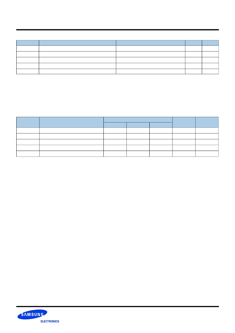
Absolute Maximum DC Ratings
Note :
1. Stresses greater than those listed under “Absolute Maximum Ratings” may cause permanent damage to the device. This is a stress rating only and
functional operation of the device at these or any other conditions above those indicated in the operational sections of this specification is not implied.
Exposure to absolute maximum rating conditions for extended periods may affect reliability.
2. Storage Temperature is the case surface temperature on the center/top side of the DRAM. For the measurement conditions, please refer to JESD51-2
standard.
AC & DC Operating Conditions
Recommended DC Operating Conditions (SSTL - 1.8)
Note : There is no specific device V
DD
supply voltage requirement for SSTL-1.8 compliance. However under all conditions V
DDQ
must be less than or equal
to V
DD
.
1. The value of V
REF
may be selected by the user to provide optimum noise margin in the system. Typically the value of V
REF
is expected to be about 0.5
x V
DDQ
of the transmitting device and V
REF
is expected to track variations in V
DDQ
.
2. Peak to peak AC noise on V
REF
may not exceed +/-2% V
REF
(DC).
3. V
TT
of transmitting device must track V
REF
of receiving device.
4. AC parameters are measured with V
DD
, V
DDQ
and V
DDL
tied together.
Symbol
Parameter
Rating
Units
Notes
V
DD
Voltage on V
DD
pin relative to V
SS
- 1.0 V ~ 2.3 V
V
1
V
DDQ
Voltage on V
DDQ
pin relative to V
SS
- 0.5 V ~ 2.3 V
V
1
V
DDL
Voltage on V
DDL
pin relative to V
SS
- 0.5 V ~ 2.3 V
V
1
V
IN,
V
OUT
Voltage on any pin relative to V
SS
- 0.5 V ~ 2.3 V
V
1
T
STG
Storage Temperature
-55 to +100
°
C
1, 2
Symbol
Parameter
Rating
Units
Notes
Min.
Typ.
Max.
V
DD
Supply Voltage
1.7
1.8
1.9
V
V
DDL
Supply Voltage for DLL
1.7
1.8
1.9
V
4
V
DDQ
Supply Voltage for Output
1.7
1.8
1.9
V
4
V
REF
Input Reference Voltage
0.49*V
DDQ
0.50*V
DDQ
0.51*V
DDQ
mV
1,2
V
TT
Termination Voltage
V
REF
-0.04
V
REF
V
REF
+0.04
V
3
相關PDF資料 |
PDF描述 |
|---|---|
| M393T5750CZ3-CCC | 40 characters x 2 Lines, 5x7 Dot Matric Character and Cursor |
| M393T2953CZ3-CD5 | 40 Characters x 4 Lines, 5x7 Dot Matrix Character and Cursor |
| M393T2950CZ3-CD5 | 40 Characters x 4 Lines, 5x7 Dot Matrix Character and Cursor |
| M393T5750CZ3-CD5 | 40 Characters x 4 Lines, 5x7 Dot Matrix Character and Cursor |
| M393T5750CZA-CE6 | DDR2 Registered SDRAM MODULE 240pin Registered Module based on 512Mb C-die 72-bit ECC |
相關代理商/技術參數(shù) |
參數(shù)描述 |
|---|---|
| M393T5750CZA-CE6 | 制造商:SAMSUNG 制造商全稱:Samsung semiconductor 功能描述:DDR2 Registered SDRAM MODULE 240pin Registered Module based on 512Mb C-die 72-bit ECC |
| M393T5750CZA-CE600 | 制造商:Samsung Semiconductor 功能描述:512MSDDDRII_MDDR SDRAM MODULX72BOC(LF) - Bulk |
| M393T5750CZA-CE7 | 制造商:SAMSUNG 制造商全稱:Samsung semiconductor 功能描述:DDR2 Registered SDRAM MODULE 240pin Registered Module based on 512Mb C-die 72-bit ECC |
| M393T5750EZA-CE600 | 制造商:Samsung Semiconductor 功能描述:512 DDR SDRAM MODUL X72 BOC(LF) - Trays |
| M393T6450FG0-CC | 制造商:SAMSUNG 制造商全稱:Samsung semiconductor 功能描述:DDR2 Registered SDRAM MODULE 240pin Registered Module based on 256Mb F-die 72-bit ECC |
發(fā)布緊急采購,3分鐘左右您將得到回復。