- 您現(xiàn)在的位置:買(mǎi)賣(mài)IC網(wǎng) > PDF目錄383298 > M393T5750CZA-CD5 (SAMSUNG SEMICONDUCTOR CO. LTD.) DDR2 Registered SDRAM MODULE 240pin Registered Module based on 512Mb C-die 72-bit ECC PDF資料下載
參數(shù)資料
| 型號(hào): | M393T5750CZA-CD5 |
| 廠商: | SAMSUNG SEMICONDUCTOR CO. LTD. |
| 英文描述: | DDR2 Registered SDRAM MODULE 240pin Registered Module based on 512Mb C-die 72-bit ECC |
| 中文描述: | 注冊(cè)的DDR2 SDRAM內(nèi)存模塊240針腳注冊(cè)模塊的512MB的基于C -死72位ECC |
| 文件頁(yè)數(shù): | 15/21頁(yè) |
| 文件大小: | 476K |
| 代理商: | M393T5750CZA-CD5 |
第1頁(yè)第2頁(yè)第3頁(yè)第4頁(yè)第5頁(yè)第6頁(yè)第7頁(yè)第8頁(yè)第9頁(yè)第10頁(yè)第11頁(yè)第12頁(yè)第13頁(yè)第14頁(yè)當(dāng)前第15頁(yè)第16頁(yè)第17頁(yè)第18頁(yè)第19頁(yè)第20頁(yè)第21頁(yè)
Rev. 1.2 Aug. 2005
512MB, 1GB, 2GB Registered DIMMs
DDR2 SDRAM
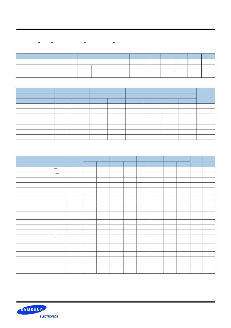
Electrical Characteristics & AC Timing for DDR2-800/667/533/400
(0
°
C < T
OPER
< 95
°
C; V
DDQ
= 1.8V + 0.1V; V
DD
= 1.8V + 0.1V)
Refresh Parameters by Device Density
Speed Bins and CL, tRCD, tRP, tRC and tRAS for Corresponding Bin
Speed
DDR2-800(E7)
Timing Parameters by Speed Grade
(Refer to notes for informations related to this table at the bottom)
Parameter
Symbol
256Mb
512Mb
1Gb
2Gb
4Gb
Units
Refresh to active/Refresh command time
tRFC
75
105
127.5
195
327.5
ns
Average periodic refresh interval
tREFI
0
°
C
≤
T
CASE
≤
85
°
C
7.8
7.8
7.8
7.8
7.8
μ
s
85
°
C
<
T
CASE
≤
95
°
C
3.9
3.9
3.9
3.9
3.9
μ
s
DDR2-667(E6)
DDR2-533(D5)
DDR2-400(CC)
Units
Bin
(CL - tRCD - tRP)
5 - 5 - 5
5 - 5 - 5
4 - 4 - 4
3 - 3 - 3
Parameter
min
max
min
max
min
max
min
max
tCK, CL=3
5
8
5
8
5
8
5
8
ns
tCK, CL=4
3.75
8
3.75
8
3.75
8
5
8
ns
tCK, CL=5
2.5
8
3
8
3.75
8
-
-
ns
tRCD
12.5
-
15
-
15
-
15
-
ns
tRP
12.5
-
15
-
15
-
15
-
ns
tRC
51.5
-
54
-
55
-
55
-
ns
tRAS
39
70000
39
70000
40
70000
40
70000
ns
Parameter
Symbol
DDR2-800
DDR2-667
DDR2-533
DDR2-400
Units
Notes
min
max
min
max
min
max
min
max
DQ output access time from CK/CK
tAC
- 400
400
-450
+450
-500
+500
-600
+600
ps
DQS output access time from CK/CK
tDQSCK
- 350
350
-400
+400
-450
+450
-500
+500
ps
CK high-level width
tCH
0.45
0.55
0.45
0.55
0.45
0.55
0.45
0.55
tCK
CK low-level width
tCL
0.45
0.55
0.45
0.55
0.45
0.55
0.45
0.55
tCK
CK half period
tHP
min(tCL,t
CH)
x
min(tCL,
tCH)
x
min(tCL,
tCH)
x
min(tCL,
tCH)
x
ps
Clock cycle time, CL=x
tCK
2500
8000
3000
8000
3750
8000
5000
8000
ps
DQ and DM input hold time
tDH(base)
125
x
175
x
225
x
275
x
ps
DQ and DM input setup time
tDS(base)
50
x
100
x
100
x
150
x
ps
Control & Address input pulse width for
each input
tIPW
0.6
x
0.6
x
0.6
x
0.6
x
tCK
DQ and DM input pulse width for each input tDIPW
0.35
x
0.35
x
0.35
x
0.35
x
tCK
Data-out high-impedance time from CK/CK tHZ
x
tAC max
x
tAC max
x
tAC max
x
tAC max
ps
DQS low-impedance time from CK/CK
tLZ(DQS)
tAC min
tAC max
tAC min
tAC max
tAC min
tAC max
tAC min
tAC max
ps
DQ low-impedance time from CK/CK
tLZ(DQ)
2* tAC
min
tAC max
2*tAC
min
tAC max
2* tACmin
tAC max
2* tACmin
tAC max
ps
DQS-DQ skew for DQS and associated DQ
signals
tDQSQ
x
200
x
240
x
300
x
350
ps
DQ hold skew factor
tQHS
x
300
x
340
x
400
x
450
ps
DQ/DQS output hold time from DQS
tQH
tHP -
tQHS
x
tHP -
tQHS
x
tHP -
tQHS
x
tHP -
tQHS
x
ps
First DQS latching transition to associated
clock edge
tDQSS
- 0.25
0.25
-0.25
0.25
-0.25
0.25
-0.25
0.25
tCK
相關(guān)PDF資料 |
PDF描述 |
|---|---|
| M393T5750CZ3-CCC | 40 characters x 2 Lines, 5x7 Dot Matric Character and Cursor |
| M393T2953CZ3-CD5 | 40 Characters x 4 Lines, 5x7 Dot Matrix Character and Cursor |
| M393T2950CZ3-CD5 | 40 Characters x 4 Lines, 5x7 Dot Matrix Character and Cursor |
| M393T5750CZ3-CD5 | 40 Characters x 4 Lines, 5x7 Dot Matrix Character and Cursor |
| M393T5750CZA-CE6 | DDR2 Registered SDRAM MODULE 240pin Registered Module based on 512Mb C-die 72-bit ECC |
相關(guān)代理商/技術(shù)參數(shù) |
參數(shù)描述 |
|---|---|
| M393T5750CZA-CE6 | 制造商:SAMSUNG 制造商全稱(chēng):Samsung semiconductor 功能描述:DDR2 Registered SDRAM MODULE 240pin Registered Module based on 512Mb C-die 72-bit ECC |
| M393T5750CZA-CE600 | 制造商:Samsung Semiconductor 功能描述:512MSDDDRII_MDDR SDRAM MODULX72BOC(LF) - Bulk |
| M393T5750CZA-CE7 | 制造商:SAMSUNG 制造商全稱(chēng):Samsung semiconductor 功能描述:DDR2 Registered SDRAM MODULE 240pin Registered Module based on 512Mb C-die 72-bit ECC |
| M393T5750EZA-CE600 | 制造商:Samsung Semiconductor 功能描述:512 DDR SDRAM MODUL X72 BOC(LF) - Trays |
| M393T6450FG0-CC | 制造商:SAMSUNG 制造商全稱(chēng):Samsung semiconductor 功能描述:DDR2 Registered SDRAM MODULE 240pin Registered Module based on 256Mb F-die 72-bit ECC |
發(fā)布緊急采購(gòu),3分鐘左右您將得到回復(fù)。