- 您現(xiàn)在的位置:買賣IC網(wǎng) > PDF目錄370847 > M37640E8FS (Mitsubishi Electric Corporation) SINGLE-CHIP 8-BIT CMOS MICROCOMPUTER PDF資料下載
參數(shù)資料
| 型號: | M37640E8FS |
| 廠商: | Mitsubishi Electric Corporation |
| 英文描述: | SINGLE-CHIP 8-BIT CMOS MICROCOMPUTER |
| 中文描述: | 單芯片8位CMOS微機 |
| 文件頁數(shù): | 74/96頁 |
| 文件大?。?/td> | 1477K |
| 代理商: | M37640E8FS |
第1頁第2頁第3頁第4頁第5頁第6頁第7頁第8頁第9頁第10頁第11頁第12頁第13頁第14頁第15頁第16頁第17頁第18頁第19頁第20頁第21頁第22頁第23頁第24頁第25頁第26頁第27頁第28頁第29頁第30頁第31頁第32頁第33頁第34頁第35頁第36頁第37頁第38頁第39頁第40頁第41頁第42頁第43頁第44頁第45頁第46頁第47頁第48頁第49頁第50頁第51頁第52頁第53頁第54頁第55頁第56頁第57頁第58頁第59頁第60頁第61頁第62頁第63頁第64頁第65頁第66頁第67頁第68頁第69頁第70頁第71頁第72頁第73頁當(dāng)前第74頁第75頁第76頁第77頁第78頁第79頁第80頁第81頁第82頁第83頁第84頁第85頁第86頁第87頁第88頁第89頁第90頁第91頁第92頁第93頁第94頁第95頁第96頁

74
Ver 1.4
MITSUBISHI MICROCOMPUTERS
7640 Group
SINGLE-CHIP 8-BIT CMOS MICROCOMPUTER
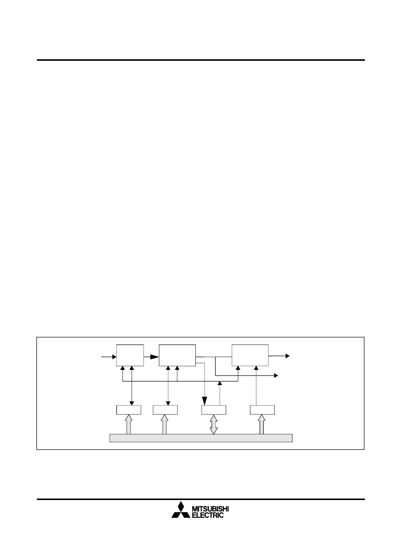
1.24.1 Frequency Synthesizer Circuit
The Frequency Synthesizer Circuit generates a 48MHz
clock needed by the USB block and a clock f
SYN
that
are both a multiple of the external input reference
clock f
IN
. A block diagram of the circuit is shown in
Figure 1.91.
The frequency synthesizer consists of a prescaler, fre-
quency multiplier macro, a frequency divider macro,
and four registers, namely FSM1, FSM2, FSC and
FSD. Two multiply registers (FSM1, FSM2) control the
frequency multiply amount. Clock f
IN
is prescaled us-
ing FSM2 to generate f
PIN
. f
PIN
is multiplied using
FSM1 to generate an f
VCO
clock which is then divided
using FSD to produce the clock f
SYN
. The f
VCO
clock
is optimized for 48 MHz operation and is buffered and
sent out of the frequency synthesizer block as signal
f
USB
. This signal is used by the USB block. The clock
block diagram is shown in Figure 1.92.
Clock f
PIN
is a divided down version of clock f
IN
, which
can be either f(X
in
) or f(XC
in
). The default clock after re-
set is fXin. The relationship between f
PIN
and the clock
input to the prescaler (f
IN
) is as follows:
f
PIN
= f
IN
/2(n+1) where n is a decimal number between
0 and 254. (See Figure 1.95).
Setting FSM2 to 255 disables the prescaler and f
PIN
=
f
IN
.
Data Bus
FSM2
FSM1
FSC
FSD
006E
006D
006C
006F
Frequency
Multiplier
Frequency
Divider
8
LS
Bit
f
IN
f
VCO
f
SYN
f
USB
Prescaler
8
f
PIN
The relationship between f
PIN
, f
VCO
, f
SYN
, and f
USB
is
as follows:
f
VCO
= f
PIN
x 2(n+1) where n is the decimal equivalent
of the value loaded in FSM1. (See Figure 1.94).
n must be chosen such that f
VCO
equals 48 MHz.
f
SYN
= f
VCO
/ 2(m+1) where m is the decimal equiva-
lent of the value loaded in FSD. (See Figure 1.96).
Setting m=255 disables the divider and disables f
SYN
.
f
USB
is a buffered version of f
VCO
, i.e., FSD has no ef-
fect on f
USB
.
Setting USB control register bit 5 to “0” disables f
USB
by tri-stating the buffer.
The FSC0 bit in the FSC Register (FSC) enables the
frequency synthesizer block. When disabled (FSC0 =
“0”), f
VCO
is held at either a high or low state. When
the frequency synthesizer control bit is active (FSC0
= “1”), a lock status (LS = “1”) indicates that f
SYN
and
fVCO are the correct frequency. The LS and FSCO
control bits in the FSC register are shown in Figure
1.93.
When using the frequency synthesizer, a low-pass fil-
ter must be connected to the LPF pin.
Once the frequency synthesizer is enabled, a delay of
2-5ms is recommended before the output of the fre-
quency synthesizer is used. This is done to allow the
output to stabilize. It is also recommended that none
of the registers be modified once the frequency syn-
thesizer is enabled as it will cause the output to be
temporarily (2-5ms) unstable.
Fig. 1.91. Frequency Synthesizer Circuit
相關(guān)PDF資料 |
PDF描述 |
|---|---|
| M37640M8-XXXFP | SINGLE CHIP 8 BIT CMOS MICROCOMPUTER |
| M37640M8-111FP | SINGLE-CHIP 8-BIT CMOS MICROCOMPUTER |
| M37640M8-126FP | SINGLE-CHIP 8-BIT CMOS MICROCOMPUTER |
| M37640E8 | SINGLE-CHIP 8-BIT CMOS MICROCONTROLLER |
| M37641F8-XXXFP | SINGLE-CHIP 8-BIT CMOS MICROCOMPUTER |
相關(guān)代理商/技術(shù)參數(shù) |
參數(shù)描述 |
|---|---|
| M37640M4T | 制造商:MITSUBISHI 制造商全稱:Mitsubishi Electric Semiconductor 功能描述:SINGLE-CHIP 8-BIT CMOS MICROCOMPUTER |
| M37640M8-111FP | 制造商:MITSUBISHI 制造商全稱:Mitsubishi Electric Semiconductor 功能描述:SINGLE-CHIP 8-BIT CMOS MICROCOMPUTER |
| M37640M8-126FP | 制造商:MITSUBISHI 制造商全稱:Mitsubishi Electric Semiconductor 功能描述:SINGLE-CHIP 8-BIT CMOS MICROCOMPUTER |
| M37640M8-XXXFP | 制造商:MITSUBISHI 制造商全稱:Mitsubishi Electric Semiconductor 功能描述:SINGLE CHIP 8 BIT CMOS MICROCOMPUTER |
| M37641F8E8-XXXFP | 制造商:RENESAS 制造商全稱:Renesas Technology Corp 功能描述:SINGLE-CHIP 8-BIT CMOS MICROCOMPUTER |
發(fā)布緊急采購,3分鐘左右您將得到回復(fù)。