- 您現(xiàn)在的位置:買賣IC網(wǎng) > PDF目錄370845 > M37510M7156FP (Mitsubishi Electric Corporation) SINGLE-CHIP 8-BIT CMOS MICROCOMPUTER PDF資料下載
參數(shù)資料
| 型號(hào): | M37510M7156FP |
| 廠商: | Mitsubishi Electric Corporation |
| 英文描述: | SINGLE-CHIP 8-BIT CMOS MICROCOMPUTER |
| 中文描述: | 單芯片8位CMOS微機(jī) |
| 文件頁(yè)數(shù): | 15/43頁(yè) |
| 文件大小: | 614K |
| 代理商: | M37510M7156FP |
第1頁(yè)第2頁(yè)第3頁(yè)第4頁(yè)第5頁(yè)第6頁(yè)第7頁(yè)第8頁(yè)第9頁(yè)第10頁(yè)第11頁(yè)第12頁(yè)第13頁(yè)第14頁(yè)當(dāng)前第15頁(yè)第16頁(yè)第17頁(yè)第18頁(yè)第19頁(yè)第20頁(yè)第21頁(yè)第22頁(yè)第23頁(yè)第24頁(yè)第25頁(yè)第26頁(yè)第27頁(yè)第28頁(yè)第29頁(yè)第30頁(yè)第31頁(yè)第32頁(yè)第33頁(yè)第34頁(yè)第35頁(yè)第36頁(yè)第37頁(yè)第38頁(yè)第39頁(yè)第40頁(yè)第41頁(yè)第42頁(yè)第43頁(yè)

15
7510 Group
SINGLE-CHIP 8-BIT CMOS MICROCOMPUTER
MITSUBISHI MICROCOMPUTERS
responding to that timer is set to “1”.
Read and write operation on 16-bit timer must be performed for
both high and low-order bytes. When reading a 16-bit timer, read
the high-order byte first. When writing to a 16-bit timer, write the
low-order byte first. The 16-bit timer cannot perform the correct op-
eration when reading during the write operation, or when writing
during the read operation.
Timer X
Timer X is a 16-bit timer that can be selected in one of four modes
and can be controlled the timer X write by setting the timer X
mode register.
Timer mode
The timer counts f(X
IN
)/16 (or f(X
CIN
)/16, if the selected system
clock
φ
is f(X
CIN
)/2).
Pulse output mode
Each time the timer underflows, a signal output from the CNTR
0
pin is inverted. Except for this, the operation in pulse output mode
is the same as in timer mode. When using a timer in this mode, set
the corresponding port P4
2
direction register to output mode.
Event counter mode
The timer counts signals input through the CNTR
0
pin. Except for
this, the operation in event counter mode is the same as in timer
mode.
Pulse width measurement mode
The count source is f(X
IN
)/16 (or f(X
CIN
)/16, if the selected system
clock
φ
is f(X
CIN
)/2). If CNTR
0
active edge selection bit is “0”, the
timer counts while the input signal of CNTR
0
pin is at “H”. If it is
“1”, the timer counts while the input signal of CNTR
0
pin is at “L”.
Timer X Write Control
If the timer X write control bit is “0”, when the value is written in the
address of timer X, the value is loaded in the timer X and the latch
at the same time.
If the timer X write control bit is “1”, when the value is written in the
address of timer X, the value is loaded only in the latch. The value
in the latch is loaded in timer X after timer X underflows.
If the value is written in latch only, unexpected value may be set in
the high-order counter when the writing in high-order latch and the
underflow of timer X are performed at the same timing.
Note on CNTR
0
Interrupt Active Edge
Selection
CNTR
0
interrupt active edge depends on the CNTR
0
active edge
selection bit.
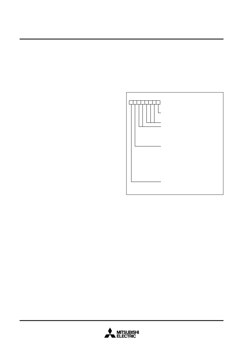
Fig. 10 Structure of timer X mode register
Timer X write control bit
0 : Write data in latch and timer
1 : Write data in latch only
Not used (Always write “0” )
Timer X operation mode bits
b5 b4
0 0 : Timer mode
0 1 : Pulse output mode
1 0 : Event counter mode
1 1 : Pulse width measurement mode
CNTR
0
active edge selection bit
0 : Count at rising edge in event counter mode
Start from “H” output in pulse output mode
Measure “H” pulse width in pulse width
measurement mode
Falling edge active for CNTR
0
interrupt
1 : Count at falling edge in event counter mode
Start from “L” output in pulse output mode
Measure “L” pulse width in pulse width
measurement mode
Rising edge active for CNTR
0
interrupt
Timer X stop control bit
0 : Count start
1 : Count stop
b7
Timer X mode register
(TXM : address 0027
16
)
b0
相關(guān)PDF資料 |
PDF描述 |
|---|---|
| M37510M8156FP | SINGLE-CHIP 8-BIT CMOS MICROCOMPUTER |
| M37510 | Single Chip 8 Bits CMOS Microcomputer(8位單片機(jī)) |
| M37510M6156FPEF | SINGLE-CHIP 8-BIT CMOS MICROCOMPUTER |
| M37515M4-C05HP | SINGLE-CHIP 8-BIT CMOS MICROCOMPUTER |
| M37515M4-C07HP | SINGLE-CHIP 8-BIT CMOS MICROCOMPUTER |
相關(guān)代理商/技術(shù)參數(shù) |
參數(shù)描述 |
|---|---|
| M37510M8156FP | 制造商:MITSUBISHI 制造商全稱:Mitsubishi Electric Semiconductor 功能描述:SINGLE-CHIP 8-BIT CMOS MICROCOMPUTER |
| M37512F8HHP | 制造商:RENESAS 制造商全稱:Renesas Technology Corp 功能描述:SINGLE-CHIP 8-BIT CMOS MICROCOMPUTER |
| M37512F8HP | 制造商:RENESAS 制造商全稱:Renesas Technology Corp 功能描述:SINGLE-CHIP 8-BIT CMOS MICROCOMPUTER |
| M37512F8H-XXXHP | 制造商:RENESAS 制造商全稱:Renesas Technology Corp 功能描述:SINGLE-CHIP 8-BIT CMOS MICROCOMPUTER |
| M37512F8-XXXHP | 制造商:RENESAS 制造商全稱:Renesas Technology Corp 功能描述:SINGLE-CHIP 8-BIT CMOS MICROCOMPUTER |
發(fā)布緊急采購(gòu),3分鐘左右您將得到回復(fù)。