- 您現(xiàn)在的位置:買賣IC網(wǎng) > PDF目錄370845 > M37481M8T-297FP (Mitsubishi Electric Corporation) SINGLE-CHIP 8-BIT CMOS MICROCOMPUTER PDF資料下載
參數(shù)資料
| 型號: | M37481M8T-297FP |
| 廠商: | Mitsubishi Electric Corporation |
| 英文描述: | SINGLE-CHIP 8-BIT CMOS MICROCOMPUTER |
| 中文描述: | 單芯片8位CMOS微機 |
| 文件頁數(shù): | 13/97頁 |
| 文件大?。?/td> | 1076K |
| 代理商: | M37481M8T-297FP |
第1頁第2頁第3頁第4頁第5頁第6頁第7頁第8頁第9頁第10頁第11頁第12頁當前第13頁第14頁第15頁第16頁第17頁第18頁第19頁第20頁第21頁第22頁第23頁第24頁第25頁第26頁第27頁第28頁第29頁第30頁第31頁第32頁第33頁第34頁第35頁第36頁第37頁第38頁第39頁第40頁第41頁第42頁第43頁第44頁第45頁第46頁第47頁第48頁第49頁第50頁第51頁第52頁第53頁第54頁第55頁第56頁第57頁第58頁第59頁第60頁第61頁第62頁第63頁第64頁第65頁第66頁第67頁第68頁第69頁第70頁第71頁第72頁第73頁第74頁第75頁第76頁第77頁第78頁第79頁第80頁第81頁第82頁第83頁第84頁第85頁第86頁第87頁第88頁第89頁第90頁第91頁第92頁第93頁第94頁第95頁第96頁第97頁

13
MITSUBISHI MICROCOMPUTERS
7480/7481 GROUP
SINGLE-CHIP 8-BIT CMOS MICROCOMPUTER
PRELIMINARY
Notice: This is not a final specification.
Some parametric limits are subject to change.
[Pull-up Control Registers]
Ports P0 and P1 are provided with a programmable pull-up tran-
sistor. When “1” is written to the pull-up control register and the
direction register is in the input mode, the pull-up transistor turns
on, and the port is pulled up.
I
Notes on Use for STP Instruction
When the 7480/7481 group is executing an STP instruction, apply
0 V or the same voltage as Vcc to the following pins.
If an intermediate voltage is applied to these pins, a through-cur-
rent flows to the input gates and the power current increases.
P4, P5, P3, P1
6
, P1
4
[Port P4P5 Input Control Register]
When ports P4
2
, P4
3
and P5 of the 7481 group are selected for in-
put, clear the corresponding direction register to “0” and set “1” to
the corresponding bit of the port P4P5 input control register.
Ports P4
2
, P4
3
and P5 are not included in the 7480 group. Fix
each bit of the port P4P5 input control register to “0”.
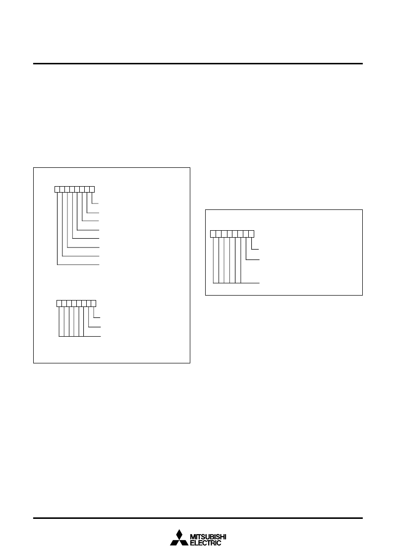
Fig. 10 Structure of pull-up control register
I/O Ports
[Direction Registers]
The I/O ports have direction registers which determine the input/
output direction of each pin in units of bit. When a bit of the direc-
tion register is set to “1”, the corresponding pin becomes an output
port. When the bit is cleared to “0”, it becomes an input port.
If data is read from a pin configured as output, the value of the
port latch is read rather than the value of this pin.
A pin configured as input becomes floating and its value can be
read. If data is written to a pin, it is written to the port latch, but the
pin remains floating.
Fig. 11 Structure of port P4P5 input control register
Port P4P5 input control register
(P4P5CON : address 00D2
16
)
P4
2
, P4
3
input control bit
P5 input control bit
(For the 7480 group) Set this bit to “0”.
(For the 7481 group) Set this bit to “1”.
b7
b0
Not used (“0” at read)
Port P1 pull-up control register
(P1PCON : address 00D1
16
)
P1
3
– P1
0
pull-up control bit
P1
7
– P1
4
pull-up control bit
b7
b0
Port P0 pull-up control register
(P0PCON
: address 00D0
16
)
P0
0
pull-up control bit
P0
1
pull-up control bit
P0
2
pull-up control bit
P0
3
pull-up control bit
P0
4
pull-up control bit
P0
5
pull-up control bit
P0
6
pull-up control bit
P0
7
pull-up control bit
b7
b0
0 : Pull-up transistor OFF
1 : Pull-up transistor ON
0 : Pull-up transistor OFF
1 : Pull-up transistor ON
Not used (undefined at read)
相關PDF資料 |
PDF描述 |
|---|---|
| M37480E8SP | SINGLE-CHIP 8-BIT CMOS MICROCOMPUTER |
| M37481E8SP | SINGLE-CHIP 8-BIT CMOS MICROCOMPUTER |
| M37481E8SS | SINGLE-CHIP 8-BIT CMOS MICROCOMPUTER |
| M37481E8T | SINGLE-CHIP 8-BIT CMOS MICROCOMPUTER |
| M37481MXT | SINGLE-CHIP 8-BIT CMOS MICROCOMPUTER |
相關代理商/技術參數(shù) |
參數(shù)描述 |
|---|---|
| M37481M8T-XXXFP | 制造商:RENESAS 制造商全稱:Renesas Technology Corp 功能描述:8-BIT SINGLE-CHIP MICROCOMPUTER 740 FAMILY / 7470 SERIES |
| M37481M8T-XXXSP | 制造商:RENESAS 制造商全稱:Renesas Technology Corp 功能描述:SINGLE-CHIP 8-BIT CMOS MICROCOMPUTER |
| M37481M8-XXXFP | 制造商:RENESAS 制造商全稱:Renesas Technology Corp 功能描述:8-BIT SINGLE-CHIP MICROCOMPUTER 740 FAMILY / 7470 SERIES |
| M37481M8-XXXSP | 制造商:RENESAS 制造商全稱:Renesas Technology Corp 功能描述:8-BIT SINGLE-CHIP MICROCOMPUTER 740 FAMILY / 7470 SERIES |
| M37481MT-088FP | 制造商:MITSUBISHI 制造商全稱:Mitsubishi Electric Semiconductor 功能描述:SINGLE-CHIP 8-BIT CMOS MICROCOMPUTER |
發(fā)布緊急采購,3分鐘左右您將得到回復。