- 您現(xiàn)在的位置:買賣IC網(wǎng) > PDF目錄67762 > M37478E8-XXXSP 8-BIT, OTPROM, MICROCONTROLLER, PDIP42 PDF資料下載
參數(shù)資料
| 型號: | M37478E8-XXXSP |
| 元件分類: | 微控制器/微處理器 |
| 英文描述: | 8-BIT, OTPROM, MICROCONTROLLER, PDIP42 |
| 封裝: | 0.600 INCH, 1.78 MM PITCH, SHRINK, PLASTIC, DIP-42 |
| 文件頁數(shù): | 228/353頁 |
| 文件大?。?/td> | 3956K |
| 代理商: | M37478E8-XXXSP |
第1頁第2頁第3頁第4頁第5頁第6頁第7頁第8頁第9頁第10頁第11頁第12頁第13頁第14頁第15頁第16頁第17頁第18頁第19頁第20頁第21頁第22頁第23頁第24頁第25頁第26頁第27頁第28頁第29頁第30頁第31頁第32頁第33頁第34頁第35頁第36頁第37頁第38頁第39頁第40頁第41頁第42頁第43頁第44頁第45頁第46頁第47頁第48頁第49頁第50頁第51頁第52頁第53頁第54頁第55頁第56頁第57頁第58頁第59頁第60頁第61頁第62頁第63頁第64頁第65頁第66頁第67頁第68頁第69頁第70頁第71頁第72頁第73頁第74頁第75頁第76頁第77頁第78頁第79頁第80頁第81頁第82頁第83頁第84頁第85頁第86頁第87頁第88頁第89頁第90頁第91頁第92頁第93頁第94頁第95頁第96頁第97頁第98頁第99頁第100頁第101頁第102頁第103頁第104頁第105頁第106頁第107頁第108頁第109頁第110頁第111頁第112頁第113頁第114頁第115頁第116頁第117頁第118頁第119頁第120頁第121頁第122頁第123頁第124頁第125頁第126頁第127頁第128頁第129頁第130頁第131頁第132頁第133頁第134頁第135頁第136頁第137頁第138頁第139頁第140頁第141頁第142頁第143頁第144頁第145頁第146頁第147頁第148頁第149頁第150頁第151頁第152頁第153頁第154頁第155頁第156頁第157頁第158頁第159頁第160頁第161頁第162頁第163頁第164頁第165頁第166頁第167頁第168頁第169頁第170頁第171頁第172頁第173頁第174頁第175頁第176頁第177頁第178頁第179頁第180頁第181頁第182頁第183頁第184頁第185頁第186頁第187頁第188頁第189頁第190頁第191頁第192頁第193頁第194頁第195頁第196頁第197頁第198頁第199頁第200頁第201頁第202頁第203頁第204頁第205頁第206頁第207頁第208頁第209頁第210頁第211頁第212頁第213頁第214頁第215頁第216頁第217頁第218頁第219頁第220頁第221頁第222頁第223頁第224頁第225頁第226頁第227頁當前第228頁第229頁第230頁第231頁第232頁第233頁第234頁第235頁第236頁第237頁第238頁第239頁第240頁第241頁第242頁第243頁第244頁第245頁第246頁第247頁第248頁第249頁第250頁第251頁第252頁第253頁第254頁第255頁第256頁第257頁第258頁第259頁第260頁第261頁第262頁第263頁第264頁第265頁第266頁第267頁第268頁第269頁第270頁第271頁第272頁第273頁第274頁第275頁第276頁第277頁第278頁第279頁第280頁第281頁第282頁第283頁第284頁第285頁第286頁第287頁第288頁第289頁第290頁第291頁第292頁第293頁第294頁第295頁第296頁第297頁第298頁第299頁第300頁第301頁第302頁第303頁第304頁第305頁第306頁第307頁第308頁第309頁第310頁第311頁第312頁第313頁第314頁第315頁第316頁第317頁第318頁第319頁第320頁第321頁第322頁第323頁第324頁第325頁第326頁第327頁第328頁第329頁第330頁第331頁第332頁第333頁第334頁第335頁第336頁第337頁第338頁第339頁第340頁第341頁第342頁第343頁第344頁第345頁第346頁第347頁第348頁第349頁第350頁第351頁第352頁第353頁
7470/7471/7477/7478 GROUP USER’S MANUAL
3-10
APPENDIX
3.1 Control registers
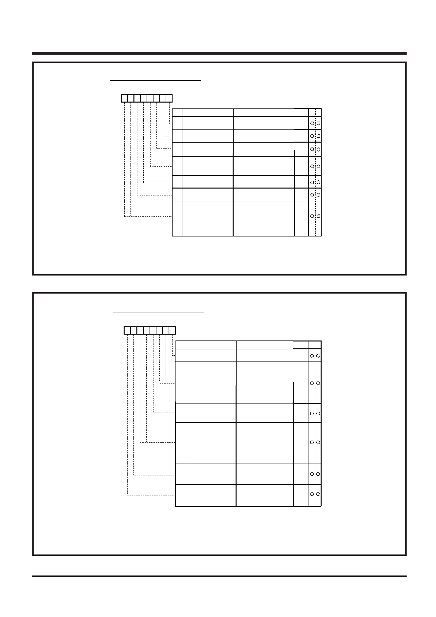
Fig. 3.1.18 Structure of Timer 34 mode register
Fig. 3.1.17 Structure of Timer 12 mode register
b7 b6 b5 b4 b3 b2 b1 b0
Name
B
Function
0
1
2
Timer 12 mode register (T12M) [Address
Timer 12 mode register
3
4
5
6, 7
b7 b6
Timer 1 count stop
bit
At reset
R
0
W
Timer 1 count
source selection bit
Timer 1 internal clock
source selection bit
P12/T0 port output
selection bit
Timer 2 count stop
bit
Timer 2 count
source selection bit
Timer 2 internal clock
source selection bits
0 : Count start
1 : Count stop
0 : Internal clock
(Note 1)
1 : P32/CNTR0 external clock
0 : f(XIN)/16 or f(XCIN)/16
1 : f(XCIN)
(Note 2)
0 : P12 port output
1 : T0(Timer 1 overflow
divided by 2)
0 : Count start
1 : Count stop
0 : Internal clock (Note 1)
1 : Timer 1 overflow signal
0 0 :
f(XIN)/16 or f(XCIN)/16
0 1 :
f(XIN)/64 or f(XCIN)/64
1 0 :
f(XIN)/128 or f(XCIN)/128
1 1 :
f(XIN)/256 or f(XCIN)/256
(Note 3)
Notes 1:
2:
3:
In the 7470/7477 group, the internal clock is f(X
Since the 7470/7477 group is not provided the sub-clock
generating circuit, f(X
Since the 7470/7477 group is not provided the sub-clock
generating circuit, f(X
00F816]
IN
)/16.
CIN
) cannot be used. Fix this bit to “0.”
CIN
) cannot be used.
b7 b6 b5 b4 b3 b2 b1 b0
Name
B
Function
0
At reset
R
0
Timer 34 mode register (T34M) [Address
Timer 34 mode register
3
0
Timer 3 count stop
bit
W
Timer 3 count
source selection bits
Timer 4 count stop
bit
Timer 4 count
source selection bits
Timer 4 pulse width
measurement mode
selection bit
0 : Count start
1 : Count stop
0 : Count start
1 : Count stop
Notes 1:
2:
When Timer 1 overflow is selected as a Timer 2
count source, the Timer 4 count source is the Timer 1
overflow regardless of the value of bit 6 of the
Timer mode register 2.
Since the 7470/7477 group is not provided the sub-clock
generating circuit, f(X CIN) cannot be used.
1, 2
b2 b1
0 0 :
f(XIN)/16 or f(XCIN)/16
0 1 :
f(XCIN)
1 0 :
Timer 1 overflow or
Timer 2 overflow
1 1 :
P33/CNTR1 external
clock
(Note 2)
b4 b3
0 0 :
Timer 3 overflow
0 1 :
f(XIN)/16 or f(XCIN)/16
1 0 :
Timer 1 overflow or
Timer 2 overflow
1 1 :
P33/CNTR1 external
clock
(Notes 1, 2)
0 : Timer mode
1 : External pulse width
measurement mode
6
0
P13/T1 port output
selection bit
0 : P13 port
1 : T1(Timer 4 overflow divided
by 2 or PWM output)
7
4, 5
00F916]
相關PDF資料 |
PDF描述 |
|---|---|
| M37478M4-XXXFP | 8-BIT, MROM, MICROCONTROLLER, PQFP56 |
| M37477E8-XXXSP | 8-BIT, OTPROM, MICROCONTROLLER, PDIP32 |
| M37477E8-XXXFP | 8-BIT, OTPROM, MICROCONTROLLER, PDSO32 |
| M37478M8-XXXFP | 8-BIT, MROM, MICROCONTROLLER, PQFP56 |
| M37477M8-XXXFP | 8-BIT, MROM, MICROCONTROLLER, PDSO32 |
相關代理商/技術參數(shù) |
參數(shù)描述 |
|---|---|
| M37478E8-XXXSP/FP | 制造商:RENESAS 制造商全稱:Renesas Technology Corp 功能描述:SINGLE-CHIP 8-BIT CMOS MICROCOMPUTER |
| M37478M2TXXXFP | 制造商:RENESAS 制造商全稱:Renesas Technology Corp 功能描述:8-BIT SINGLE-CHIP MICROCOMPUTER 740 FAMILY / 7470 SERIES |
| M37478M2TXXXSP | 制造商:RENESAS 制造商全稱:Renesas Technology Corp 功能描述:8-BIT SINGLE-CHIP MICROCOMPUTER 740 FAMILY / 7470 SERIES |
| M37478M2TXXXSP/FP | 制造商:RENESAS 制造商全稱:Renesas Technology Corp 功能描述:SINGLE-CHIP 8-BIT CMOS MICROCOMPUTER |
| M37478M4 | 制造商:MITSUBISHI 制造商全稱:Mitsubishi Electric Semiconductor 功能描述:SINGLE-CHIP 8-BIT CMOS MICROCOMPUTER |
發(fā)布緊急采購,3分鐘左右您將得到回復。