- 您現(xiàn)在的位置:買賣IC網(wǎng) > PDF目錄383296 > M366S0924FTS-C7A (SAMSUNG SEMICONDUCTOR CO. LTD.) SDRAM Unbuffered Module PDF資料下載
參數(shù)資料
| 型號: | M366S0924FTS-C7A |
| 廠商: | SAMSUNG SEMICONDUCTOR CO. LTD. |
| 英文描述: | SDRAM Unbuffered Module |
| 中文描述: | 內(nèi)存緩沖模塊 |
| 文件頁數(shù): | 5/26頁 |
| 文件大?。?/td> | 486K |
| 代理商: | M366S0924FTS-C7A |
第1頁第2頁第3頁第4頁當(dāng)前第5頁第6頁第7頁第8頁第9頁第10頁第11頁第12頁第13頁第14頁第15頁第16頁第17頁第18頁第19頁第20頁第21頁第22頁第23頁第24頁第25頁第26頁
64MB, 128MB, 256MB Unbuffered DIMM
Rev. 1.3 May 2004
SDRAM
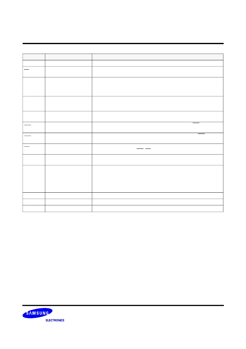
PIN CONFIGURATION DESCRIPTION
Pin
Name
Input Function
CLK
System clock
Active on the positive going edge to sample all inputs.
CS
Chip select
Disables or enables device operation by masking or enabling all inputs except
CLK, CKE and DQM
CKE
Clock enable
Masks system clock to freeze operation from the next clock cycle.
CKE should be enabled at least one cycle prior to new command.
Disable input buffers for power down in standby.
CKE should be enabled 1CLK+tss prior to valid command.
A0 ~ A11
Address
Row/column addresses are multiplexed on the same pins.
Row address : RA0 ~ RA11
Column address : (x8 : CA0 ~ CA9), (x16 : CA0 ~ CA8)
BA0 ~ BA1
Bank select address
Selects bank to be activated during row address latch time.
Selects bank for read/write during column address latch time.
RAS
Row address strobe
Latches row addresses on the positive going edge of the CLK with RAS low.
Enables row access & precharge.
CAS
Column address strobe
Latches column addresses on the positive going edge of the CLK with CAS low.
Enables column access.
WE
Write enable
Enables write operation and row precharge.
Latches data in starting from CAS, WE active.
DQM0 ~ 7
Data input/output mask
Makes data output Hi-Z, t
SHZ
after the clock and masks the output.
Blocks data input when DQM active. (Byte masking)
REGE
Register enable
The device operates in the transparent mode when REGE is low. When REGE is high,
the device operates in the registered mode. In registered mode, the Address and con-
trol inputs are latched if CLK is held at a high or low logic level. the inputs are stored in
the latch/flip-flop on the rising edge of CLK. REGE is tied to V
DD
through 10K ohm
Resistor on PCB. So if REGE of module is floating, this module will be operated as reg-
istered mode.
DQ0 ~ 63
Data input/output
Data inputs/outputs are multiplexed on the same pins.
CB0 ~ 7
Check bit
Check bits for ECC.
V
DD
/V
SS
Power supply/ground
Power and ground for the input buffers and the core logic.
相關(guān)PDF資料 |
PDF描述 |
|---|---|
| M366S1723FTS-C7A | SDRAM Unbuffered Module |
| M366S1723FTU-C7A | SDRAM Unbuffered Module |
| M374S1723FTU-C7A | SDRAM Unbuffered Module |
| M374S3323FTU-C7A | SDRAM Unbuffered Module |
| M374S3323FTS-C7A | SDRAM Unbuffered Module |
相關(guān)代理商/技術(shù)參數(shù) |
參數(shù)描述 |
|---|---|
| M366S0924FTS-C7A00 | 制造商:Samsung Semiconductor 功能描述:DRAM Module SDRAM 64Mbyte 168UDIMM Tray |
| M366S0924IUS | 制造商:SAMSUNG 制造商全稱:Samsung semiconductor 功能描述:SDRAM Product Guide |
| M366S1623DT0 | 制造商:SAMSUNG 制造商全稱:Samsung semiconductor 功能描述:PC100 Unbuffered DIMM |
| M366S1623DT0-C1H | 制造商:SAMSUNG 制造商全稱:Samsung semiconductor 功能描述:PC100 Unbuffered DIMM |
| M366S1623DT0-C1L | 制造商:SAMSUNG 制造商全稱:Samsung semiconductor 功能描述:PC100 Unbuffered DIMM |
發(fā)布緊急采購,3分鐘左右您將得到回復(fù)。