- 您現(xiàn)在的位置:買賣IC網(wǎng) > PDF目錄69011 > M34570M4-XXXFP 4-BIT, MROM, 2 MHz, MICROCONTROLLER, PDSO36 PDF資料下載
參數(shù)資料
| 型號(hào): | M34570M4-XXXFP |
| 元件分類: | 微控制器/微處理器 |
| 英文描述: | 4-BIT, MROM, 2 MHz, MICROCONTROLLER, PDSO36 |
| 封裝: | 0.450 INCH, 0.80 MM PITCH, PLASTIC, SSOP-36 |
| 文件頁數(shù): | 63/69頁 |
| 文件大小: | 687K |
| 代理商: | M34570M4-XXXFP |
第1頁第2頁第3頁第4頁第5頁第6頁第7頁第8頁第9頁第10頁第11頁第12頁第13頁第14頁第15頁第16頁第17頁第18頁第19頁第20頁第21頁第22頁第23頁第24頁第25頁第26頁第27頁第28頁第29頁第30頁第31頁第32頁第33頁第34頁第35頁第36頁第37頁第38頁第39頁第40頁第41頁第42頁第43頁第44頁第45頁第46頁第47頁第48頁第49頁第50頁第51頁第52頁第53頁第54頁第55頁第56頁第57頁第58頁第59頁第60頁第61頁第62頁當(dāng)前第63頁第64頁第65頁第66頁第67頁第68頁第69頁
System Clock
67
Under
development
Preliminary Specifications REV.1.02
Specifications in this manual are tentative and subject to change.
Mitsubishi Microcomputers
M32C/83 group
SINGLE-CHIP 16/32-BIT CMOS MICROCOMPUTER
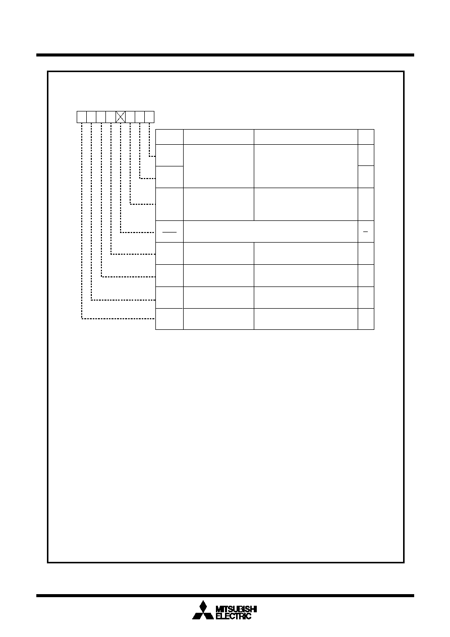
Figure 1.8.2. CM0 register
Symbol
Address
When reset
CM0
000616
0000 X0002
System clock control register 01
CM00
CM01
CM02
Clock output function
select bit2
In WAIT peripheral
function clock stop bit
Port XC switch bit
Main clock (XIN-XOUT)
stop bit5
CM04
CM05
CM06
CM07
Nothing is assigned. When write, should set to "0".
When read, its content is indeterminate.
RW
Function
Bit name
Bit
symbol
RW
0 : Main clock oscillation
1 : Main clock stop6
0 0 : I/O port P53
0 1 : fC output
1 0 : f8 output
1 1 : f32 output
0 : I/O port function
1 : XCIN-XCOUT oscilation function4
Watchdog timer
function select bit
System clock select bit8
0 : Select XIN - XOUT
1 : Select XCIN - XCOUT
0 : Watchdog timer interrupt
1 : Reset7
Notes :
1. The PRC0 bit in the PRCR register should be set to "1" (write enable) before rewriting to the CM0
register.
2. When the PM07 bit in the PM0 register is set to "0" (BCLK output), the CM01 to CM00 bits should be
set to "002". When the PM15 to PM14 bits in the PM1 register is set to "012" (ALE output to P53), the
CM01 to CM00 bits should be set to "002". When the PM07 bit is set to "1" (function selected in the
CM01 to CM00 bits) in microprocessor or memory expansion mode, the CM01 to CM00 bits should
be set to "002" to output "L" from port P53 (port P53 does not function as an I/O port).
3. fc32 is not stopped. When setting the CM02 bit to "1", the PLL clock cannot be used in wait mode.
4. When setting the CM04 bit to "1" (XCIN-XCOUT oscillation), the PD8_7 to PD8_6 bits should be set to
"002" (with port P87 and P86 input mode) and the PU25 bit in the PUR2 register be set to "0" (no pull-
up).
5. To enter low-power consumption mode or ring oscillator low power consumption mode, the CM05 bit
stops the main clock. The CM05 bit cannot detect whether the main clock stops or not. To stop the
main clock, the CM05 bit should be set to "1" after the CM07 bit is set to "1" with a stable sub clock
oscillation or after the CM21 bit in the CM2 register is set to "1" (ring oscillator clock). When setting
the CM05 bit to "1" (main clock stop), XOUT is set to "H". Also, an internal feedback resistance
remains ON. XIN is pulled up to XOUT ("H" level) via feedback resistance.
6. When setting the CM05 bit to "1", the MCD4 to MCD0 bits in the MCD register are set to "010002"
(divide-by-8 mode). In ring oscillation mode, the MCD register is not divided by eight even if XIN-Xout
is terminated by the CM05 bit.
7. Once the CM06 bit is set to "1", it cannot be set "0" by program.
8. After setting the CM04 bit to "1" with a stable sub clock oscillation, the CM07 bit should be changed
"0" to "1".
After setting the CM05 bit to "0" with a stable main clock oscillation, the CM07 bit should be changed
"1" to "0".
Avoid setting the CM07 bit and CM04 or CM05 bits simultaneously.
b7
b6
b5
b4
b3
b2
b1
b0
b1 b0
0 : Peripheral clock does not stop in
wait mode
1 : Peripheral clock stops in wait
mode3
相關(guān)PDF資料 |
PDF描述 |
|---|---|
| M34570M8-XXXFP | 4-BIT, MROM, MICROCONTROLLER, PDSO36 |
| M34570EDFP | 4-BIT, OTPROM, MICROCONTROLLER, PDSO36 |
| M34584EDFP | 4-BIT, OTPROM, 6 MHz, MICROCONTROLLER, PDSO42 |
| M34584MD-XXXFP | 4-BIT, MROM, 6 MHz, MICROCONTROLLER, PDSO42 |
| M35017-001FP | 24 X 10 CHARACTERS CRT CHAR DSPL CTLR, PDSO20 |
相關(guān)代理商/技術(shù)參數(shù) |
參數(shù)描述 |
|---|---|
| M34570M8 | 制造商:MITSUBISHI 制造商全稱:Mitsubishi Electric Semiconductor 功能描述:SINGLE-CHIP 4-BIT CMOS MICROCOMPUTER |
| M34570M8-117FP | 制造商:MITSUBISHI 制造商全稱:Mitsubishi Electric Semiconductor 功能描述:SINGLE-CHIP 4-BIT CMOS MICROCOMPUTER |
| M34570M8-XXXFP | 制造商:RENESAS 制造商全稱:Renesas Technology Corp 功能描述:SINGLE-CHIP 4-BIT CMOS MICROCOMPUTER |
| M34570MD | 制造商:MITSUBISHI 制造商全稱:Mitsubishi Electric Semiconductor 功能描述:SINGLE-CHIP 4-BIT CMOS MICROCOMPUTER |
| M34570MD-XXXFP | 制造商:RENESAS 制造商全稱:Renesas Technology Corp 功能描述:SINGLE-CHIP 4-BIT CMOS MICROCOMPUTER |
發(fā)布緊急采購,3分鐘左右您將得到回復(fù)。