- 您現(xiàn)在的位置:買賣IC網(wǎng) > PDF目錄45027 > M34554MC-XXXFP 4-BIT, MROM, 6 MHz, MICROCONTROLLER, PQFP64 PDF資料下載
參數(shù)資料
| 型號(hào): | M34554MC-XXXFP |
| 元件分類: | 微控制器/微處理器 |
| 英文描述: | 4-BIT, MROM, 6 MHz, MICROCONTROLLER, PQFP64 |
| 封裝: | 14 X 14 MM, 0.80 MM PITCH, PLASTIC, QFP-64 |
| 文件頁(yè)數(shù): | 39/138頁(yè) |
| 文件大小: | 1082K |
| 代理商: | M34554MC-XXXFP |
第1頁(yè)第2頁(yè)第3頁(yè)第4頁(yè)第5頁(yè)第6頁(yè)第7頁(yè)第8頁(yè)第9頁(yè)第10頁(yè)第11頁(yè)第12頁(yè)第13頁(yè)第14頁(yè)第15頁(yè)第16頁(yè)第17頁(yè)第18頁(yè)第19頁(yè)第20頁(yè)第21頁(yè)第22頁(yè)第23頁(yè)第24頁(yè)第25頁(yè)第26頁(yè)第27頁(yè)第28頁(yè)第29頁(yè)第30頁(yè)第31頁(yè)第32頁(yè)第33頁(yè)第34頁(yè)第35頁(yè)第36頁(yè)第37頁(yè)第38頁(yè)當(dāng)前第39頁(yè)第40頁(yè)第41頁(yè)第42頁(yè)第43頁(yè)第44頁(yè)第45頁(yè)第46頁(yè)第47頁(yè)第48頁(yè)第49頁(yè)第50頁(yè)第51頁(yè)第52頁(yè)第53頁(yè)第54頁(yè)第55頁(yè)第56頁(yè)第57頁(yè)第58頁(yè)第59頁(yè)第60頁(yè)第61頁(yè)第62頁(yè)第63頁(yè)第64頁(yè)第65頁(yè)第66頁(yè)第67頁(yè)第68頁(yè)第69頁(yè)第70頁(yè)第71頁(yè)第72頁(yè)第73頁(yè)第74頁(yè)第75頁(yè)第76頁(yè)第77頁(yè)第78頁(yè)第79頁(yè)第80頁(yè)第81頁(yè)第82頁(yè)第83頁(yè)第84頁(yè)第85頁(yè)第86頁(yè)第87頁(yè)第88頁(yè)第89頁(yè)第90頁(yè)第91頁(yè)第92頁(yè)第93頁(yè)第94頁(yè)第95頁(yè)第96頁(yè)第97頁(yè)第98頁(yè)第99頁(yè)第100頁(yè)第101頁(yè)第102頁(yè)第103頁(yè)第104頁(yè)第105頁(yè)第106頁(yè)第107頁(yè)第108頁(yè)第109頁(yè)第110頁(yè)第111頁(yè)第112頁(yè)第113頁(yè)第114頁(yè)第115頁(yè)第116頁(yè)第117頁(yè)第118頁(yè)第119頁(yè)第120頁(yè)第121頁(yè)第122頁(yè)第123頁(yè)第124頁(yè)第125頁(yè)第126頁(yè)第127頁(yè)第128頁(yè)第129頁(yè)第130頁(yè)第131頁(yè)第132頁(yè)第133頁(yè)第134頁(yè)第135頁(yè)第136頁(yè)第137頁(yè)第138頁(yè)
Rev.3.00
Aug 06, 2004
page 133 of 136
REJ03B0043-0300Z
4554 Group
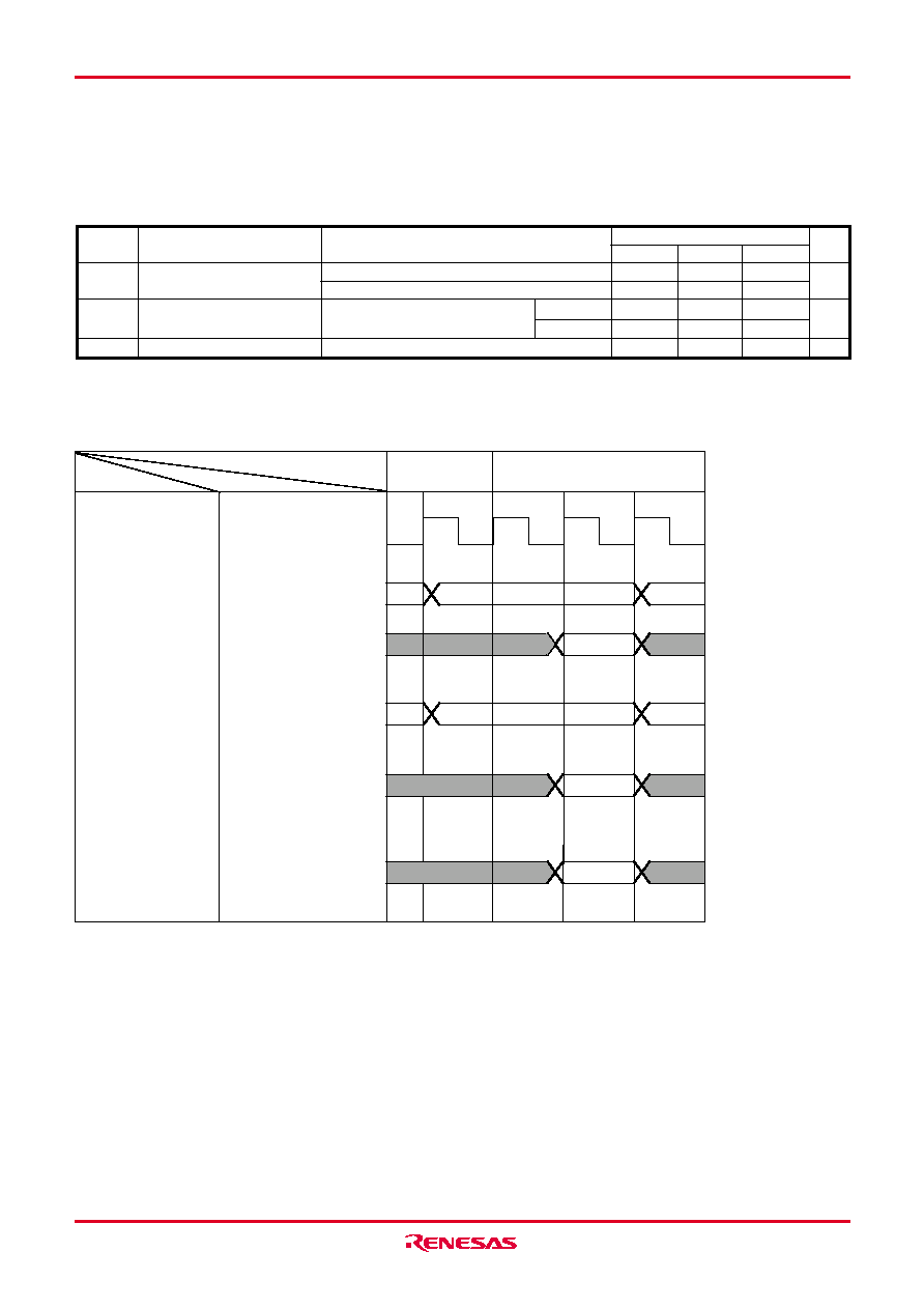
BASIC TIMING DIAGRAM
VOLTAGE DROP DETECTION CIRCUIT CHARACTERISTICS
(Ta = –20 °C to 85 °C, unless otherwise noted)
Test conditions
Ta = 25 °C
at power down
VDD = 5 V
(Note 2)
VDD = 3 V
VDD
→ (VRST–0.1 V) (Note 3)
Parameter
Detection voltage (Note 1)
Operation current
Detection time
Symbol
VRST
IRST
TRST
Limits
Unit
Min.
1.4
1.1
Typ.
1.5
50
30
0.2
Max.
1.6
1.9
100
60
1.2
V
A
ms
Notes 1: The detected voltage (VRST) is defined as the voltage when reset occurs when the supply voltage (VDD) is falling.
2: After the SVDE instruction is executed, the voltage drop detectin circuit is valid at power down mode.
3: The detection time (TRST) is defined as the time until reset occurs when the supply voltage (VDD) is falling to [VRST–0.1 V].
STCK
Parameter
Pin (signal) name
Machine cycle
MiMi+1
D0–D9
System clock
Port D output
Port D input
Ports P0, P1 output
Ports P0, P1, P2, P3
input
D0–D7
INT0, INT1
Interrupt input
P00–P03
P10–P13
P00–P03
P10–P13
P20–P23
P30–P33
相關(guān)PDF資料 |
PDF描述 |
|---|---|
| M34554EDFP | 4-BIT, OTPROM, 6 MHz, MICROCONTROLLER, PQFP64 |
| M3455AG8-XXXFP | 4-BIT, OTPROM, 6 MHz, MICROCONTROLLER, PQFP52 |
| M3455AGCFP | 4-BIT, OTPROM, 6 MHz, MICROCONTROLLER, PQFP52 |
| M3455AGC-XXXFP | 4-BIT, OTPROM, 6 MHz, MICROCONTROLLER, PQFP52 |
| M3455AG8FP | 4-BIT, OTPROM, 6 MHz, MICROCONTROLLER, PQFP52 |
相關(guān)代理商/技術(shù)參數(shù) |
參數(shù)描述 |
|---|---|
| M34556G8FP | 制造商:RENESAS 制造商全稱:Renesas Technology Corp 功能描述:SINGLE-CHIP 4-BIT CMOS MICROCOMPUTER |
| M34556G8HFP | 制造商:RENESAS 制造商全稱:Renesas Technology Corp 功能描述:SINGLE-CHIP 4-BIT CMOS MICROCOMPUTER |
| M34556M4H-XXXFP | 制造商:RENESAS 制造商全稱:Renesas Technology Corp 功能描述:SINGLE-CHIP 4-BIT CMOS MICROCOMPUTER |
| M34556M4-XXXFP | 制造商:RENESAS 制造商全稱:Renesas Technology Corp 功能描述:SINGLE-CHIP 4-BIT CMOS MICROCOMPUTER |
| M34556M8H-XXXFP | 制造商:RENESAS 制造商全稱:Renesas Technology Corp 功能描述:SINGLE-CHIP 4-BIT CMOS MICROCOMPUTER |
發(fā)布緊急采購(gòu),3分鐘左右您將得到回復(fù)。