- 您現(xiàn)在的位置:買賣IC網(wǎng) > PDF目錄67761 > M34502E4FP 4-BIT, OTPROM, MICROCONTROLLER, PDSO24 PDF資料下載
參數(shù)資料
| 型號: | M34502E4FP |
| 元件分類: | 微控制器/微處理器 |
| 英文描述: | 4-BIT, OTPROM, MICROCONTROLLER, PDSO24 |
| 封裝: | 5.30 X 10.10 MM, 0.80 MM PITCH, PLASTIC, SSOP-24 |
| 文件頁數(shù): | 51/116頁 |
| 文件大?。?/td> | 896K |
| 代理商: | M34502E4FP |
第1頁第2頁第3頁第4頁第5頁第6頁第7頁第8頁第9頁第10頁第11頁第12頁第13頁第14頁第15頁第16頁第17頁第18頁第19頁第20頁第21頁第22頁第23頁第24頁第25頁第26頁第27頁第28頁第29頁第30頁第31頁第32頁第33頁第34頁第35頁第36頁第37頁第38頁第39頁第40頁第41頁第42頁第43頁第44頁第45頁第46頁第47頁第48頁第49頁第50頁當(dāng)前第51頁第52頁第53頁第54頁第55頁第56頁第57頁第58頁第59頁第60頁第61頁第62頁第63頁第64頁第65頁第66頁第67頁第68頁第69頁第70頁第71頁第72頁第73頁第74頁第75頁第76頁第77頁第78頁第79頁第80頁第81頁第82頁第83頁第84頁第85頁第86頁第87頁第88頁第89頁第90頁第91頁第92頁第93頁第94頁第95頁第96頁第97頁第98頁第99頁第100頁第101頁第102頁第103頁第104頁第105頁第106頁第107頁第108頁第109頁第110頁第111頁第112頁第113頁第114頁第115頁第116頁
Rev.3.01
2005.02.02
page 4 of 112
REJ03B0105-0301
4502 Group
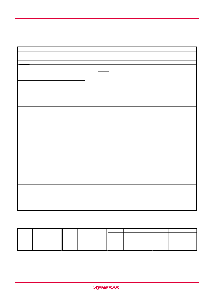
PIN DESCRIPTION
Name
Power supply
Ground
CNVSS
Reset input/output
System clock input
I/O port D
I/O port P0
I/O port P1
I/O port P2
I/O port P3
I/O port C
I/O port K
Timer input/output
Interrupt input
Analog input
Pin
VDD
VSS
CNVSS
RESET
XIN
D0–D5
P00–P03
P10–P13
P20, P21
P30, P31
Port C
Port K
CNTR
INT
AIN0–AIN3
Input/Output
—
I/O
Input
I/O
Input
Function
Connected to a plus power supply.
Connected to a 0 V power supply.
Connect CNVSS to VSS and apply “L” (0V) to CNVSS certainly.
An N-channel open-drain I/O pin for a system reset. When the watchdog timer, the
built-in power-on reset or the voltage drop detection circuit causes the system to be
reset, the RESET pin outputs “L” level.
I/O pins of the system clock generating circuit. When using a ceramic resonator, connect
it between pins XIN and XOUT. A feedback resistor is built-in between them. When using
the RC oscillation, connect a resistor and a capacitor to XIN, and leave XOUT pin open.
Each pin of port D has an independent 1-bit wide I/O function. Each pin has an out-
put latch. For input use, set the latch of the specified bit to “1.” Input is examined by
skip decision. The output structure is N-channel open-drain. Ports D2 and D3 are
equipped with a pull-up function and a key-on wakeup function. Both functions can
be switched by software.
Ports D2 and D3 are also used as ports C and K, respectively.
Port P0 serves as a 4-bit I/O port, and it can be used as inputs when the output latch
is set to “1.” The output structure is N-channel open-drain. Port P0 has a key-on
wakeup function and a pull-up function. Both functions can be switched by software.
Port P1 serves as a 4-bit I/O port, and it can be used as inputs when the output latch
is set to “1.” The output structure is N-channel open-drain. Port P1 has a key-on
wakeup function and a pull-up function. Both functions can be switched by software.
Ports P12 and P13 are also used as CNTR and INT, respectively.
Port P2 serves as a 2-bit I/O port, and it can be used as inputs when the output latch
is set to “1.” The output structure is N-channel open-drain. Port P2 has a key-on
wakeup function and a pull-up function. Both functions can be switched by software.
Ports P20 and P21 are also used as AIN0 and AIN1, respectively.
Port P3 serves as a 2-bit I/O port, and it can be used as inputs when the output latch
is set to “1.” The output structure is N-channel open-drain. Ports P30 and P31 are
also used as AIN2 and AIN3, respectively.
1-bit I/O port. Port C can be used as inputs when the output latch is set to “1.” The
output structure is N-channel open-drain. Port C has a key-on wakeup function and
a pull-up function. Both functions can be switched by software. Port C is also used
as port D2.
1-bit I/O port. Port K can be used as inputs when the output latch is set to “1.” The
output structure is N-channel open-drain. Port K has a key-on wakeup function and
a pull-up function. Both functions can be switched by software. Port K is also used
as port D3.
CNTR pin has the function to input the clock for the timer 2 event counter, and to out-
put the timer 1 or timer 2 underflow signal divided by 2. This pin is also used as port
P12.
INT pin accepts external interrupts. It has the key-on wakeup function which can be
switched by software. This pin is also used as port P13.
A/D converter analog input pins. AIN0 and AIN1 are also used as ports P20 and P21,
respectively. AIN2 and AIN3 are also used as ports P30 and P31, respectively.
Notes 1: Pins except above have just single function.
2: The input/output of D2, D3, P12 and P13 can be used even when C, K, CNTR (input) and INT are selected.
3: The input of P12 can be used even when CNTR (output) is selected.
4: The input/output of P20, P21, P30 and P31 can be used even when AIN0, AIN1, AIN2 and AIN3 are selected.
Pin
D2
D3
P12
P13
Multifunction
C
K
CNTR
INT
MULTIFUNCTION
Pin
C
K
CNTR
INT
Multifunction
D2
D3
P12
P13
Pin
P20
P21
P30
P31
Multifunction
AIN0
AIN1
AIN2
AIN3
Pin
AIN0
AIN1
AIN2
AIN3
Multifunction
P20
P21
P30
P31
XOUT
System clock output
Output
相關(guān)PDF資料 |
PDF描述 |
|---|---|
| M34502M4-XXXFP | 4-BIT, MROM, MICROCONTROLLER, PDSO24 |
| M34502M2-XXXFP | 4-BIT, MROM, MICROCONTROLLER, PDSO24 |
| M34508G4GP | 4-BIT, MROM, 6 MHz, MICROCONTROLLER, PDSO20 |
| M34508G4H-XXXFP | 4-BIT, MROM, 6 MHz, MICROCONTROLLER, PDSO20 |
| M34508G4-XXXFP | 4-BIT, MROM, 6 MHz, MICROCONTROLLER, PDSO20 |
相關(guān)代理商/技術(shù)參數(shù) |
參數(shù)描述 |
|---|---|
| M34502M2 | 制造商:RENESAS 制造商全稱:Renesas Technology Corp 功能描述:SINGLE-CHIP 4-BIT CMOS MICROCOMPUTER |
| M34502M2-XXXFP | 制造商:RENESAS 制造商全稱:Renesas Technology Corp 功能描述:SINGLE-CHIP 4-BIT CMOS MICROCOMPUTER |
| M34502M4 | 制造商:RENESAS 制造商全稱:Renesas Technology Corp 功能描述:SINGLE-CHIP 4-BIT CMOS MICROCOMPUTER |
| M34502M4-XXXFP | 制造商:RENESAS 制造商全稱:Renesas Technology Corp 功能描述:SINGLE-CHIP 4-BIT CMOS MICROCOMPUTER |
| M34506E4 | 制造商:RENESAS 制造商全稱:Renesas Technology Corp 功能描述:SINGLE-CHIP 4-BIT CMOS MICROCOMPUTER |
發(fā)布緊急采購,3分鐘左右您將得到回復(fù)。