- 您現(xiàn)在的位置:買賣IC網(wǎng) > PDF目錄67761 > M34502E4FP 4-BIT, OTPROM, MICROCONTROLLER, PDSO24 PDF資料下載
參數(shù)資料
| 型號(hào): | M34502E4FP |
| 元件分類: | 微控制器/微處理器 |
| 英文描述: | 4-BIT, OTPROM, MICROCONTROLLER, PDSO24 |
| 封裝: | 5.30 X 10.10 MM, 0.80 MM PITCH, PLASTIC, SSOP-24 |
| 文件頁數(shù): | 45/116頁 |
| 文件大?。?/td> | 896K |
| 代理商: | M34502E4FP |
第1頁第2頁第3頁第4頁第5頁第6頁第7頁第8頁第9頁第10頁第11頁第12頁第13頁第14頁第15頁第16頁第17頁第18頁第19頁第20頁第21頁第22頁第23頁第24頁第25頁第26頁第27頁第28頁第29頁第30頁第31頁第32頁第33頁第34頁第35頁第36頁第37頁第38頁第39頁第40頁第41頁第42頁第43頁第44頁當(dāng)前第45頁第46頁第47頁第48頁第49頁第50頁第51頁第52頁第53頁第54頁第55頁第56頁第57頁第58頁第59頁第60頁第61頁第62頁第63頁第64頁第65頁第66頁第67頁第68頁第69頁第70頁第71頁第72頁第73頁第74頁第75頁第76頁第77頁第78頁第79頁第80頁第81頁第82頁第83頁第84頁第85頁第86頁第87頁第88頁第89頁第90頁第91頁第92頁第93頁第94頁第95頁第96頁第97頁第98頁第99頁第100頁第101頁第102頁第103頁第104頁第105頁第106頁第107頁第108頁第109頁第110頁第111頁第112頁第113頁第114頁第115頁第116頁
Rev.3.01
2005.02.02
page 34 of 112
REJ03B0105-0301
4502 Group
(9) Operation at comparator mode
The A/D converter is set to comparator mode by setting bit 3 of the
register Q1 to “1.”
Below, the operation at comparator mode is described.
(10) Comparator register
In comparator mode, the built-in DA comparator is connected to the
8-bit comparator register as a register for setting comparison volt-
ages. The contents of register B is stored in the high-order 4 bits of
the comparator register and the contents of register A is stored in
the low-order 4 bits of the comparator register with the TADAB in-
struction.
When changing from A/D conversion mode to comparator mode,
the result of A/D conversion (register AD) is undefined.
However, because the comparator register is separated from regis-
ter AD, the value is retained even when changing from comparator
mode to A/D conversion mode. Note that the comparator register
can be written and read at only comparator mode.
If the value in the comparator register is n, the logic value of com-
parison voltage Vref generated by the built-in DA converter can be
determined from the following formula:
(11) Comparison result store flag (ADF)
In comparator mode, the ADF flag, which shows completion of A/D
conversion, stores the results of comparing the analog input volt-
age with the comparison voltage. When the analog input voltage is
lower than the comparison voltage, the ADF flag is set to “1.” The
state of ADF flag can be examined with the skip instruction
(SNZAD). Use the interrupt control register V2 to select the inter-
rupt or the skip instruction.
The ADF flag is cleared to “0” when the interrupt occurs or when
the next instruction is skipped with the skip instruction.
(12) Comparator operation start instruction
(ADST instruction)
In comparator mode, executing ADST starts the comparator oper-
ating.
The comparator stops 8 machine cycles after it has started (6
s at
f(XIN) = 4.0 MHz in high-speed mode). When the analog input volt-
age is lower than the comparison voltage, the ADF flag is set to “1.”
(13) Notes for the use of A/D conversion 1
Note the following when using the analog input pins also for ports
P2 and P3 functions:
Selection of analog input pins
Even when P20/AIN0, P21/AIN1, P30/AIN2, P31/AIN3 are set to pins
for analog input, they continue to function as ports P2 and P3 in-
put/output. Accordingly, when any of them are used as I/O port
and others are used as analog input pins, make sure to set the
outputs of pins that are set for analog input to “1.” Also, the port
input function of the pin functions as an analog input is unde-
fined.
TALA instruction
When the TALA instruction is executed, the low-order 2 bits of
register AD is transferred to the high-order 2 bits of register A, si-
multaneously, the low-order 2 bits of register A is “0.”
(14) Notes for the use of A/D conversion 2
Do not change the operating mode (both A/D conversion mode and
comparator mode) of A/D converter with the bit 3 of register Q1
while the A/D converter is operating.
When the operating mode of A/D converter is changed from the
comparator mode to A/D conversion mode with the bit 3 of register
Q1, note the following;
Clear the bit 2 of register V2 to “0” to change the operating mode
of the A/D converter from the comparator mode to A/D conver-
sion mode with the bit 3 of register Q1.
The A/D conversion completion flag (ADF) may be set when the
operating mode of the A/D converter is changed from the com-
parator mode to the A/D conversion mode. Accordingly, set a
value to the bit 3 of register Q1, and execute the SNZAD instruc-
tion to clear the ADF flag.
Logic value of comparison voltage Vref
Vref =
n
n: The value of register AD (n = 0 to 255)
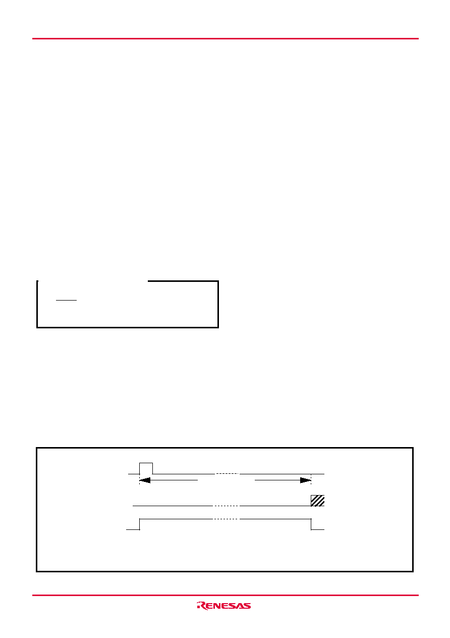
Fig. 31 Comparator operation timing chart
VDD
256
ADST instruction
Comparison result
store flag(ADF)
8 machine cycles
DAC operation signal
Comparator operation completed.
(The value of ADF is determined)
→
相關(guān)PDF資料 |
PDF描述 |
|---|---|
| M34502M4-XXXFP | 4-BIT, MROM, MICROCONTROLLER, PDSO24 |
| M34502M2-XXXFP | 4-BIT, MROM, MICROCONTROLLER, PDSO24 |
| M34508G4GP | 4-BIT, MROM, 6 MHz, MICROCONTROLLER, PDSO20 |
| M34508G4H-XXXFP | 4-BIT, MROM, 6 MHz, MICROCONTROLLER, PDSO20 |
| M34508G4-XXXFP | 4-BIT, MROM, 6 MHz, MICROCONTROLLER, PDSO20 |
相關(guān)代理商/技術(shù)參數(shù) |
參數(shù)描述 |
|---|---|
| M34502M2 | 制造商:RENESAS 制造商全稱:Renesas Technology Corp 功能描述:SINGLE-CHIP 4-BIT CMOS MICROCOMPUTER |
| M34502M2-XXXFP | 制造商:RENESAS 制造商全稱:Renesas Technology Corp 功能描述:SINGLE-CHIP 4-BIT CMOS MICROCOMPUTER |
| M34502M4 | 制造商:RENESAS 制造商全稱:Renesas Technology Corp 功能描述:SINGLE-CHIP 4-BIT CMOS MICROCOMPUTER |
| M34502M4-XXXFP | 制造商:RENESAS 制造商全稱:Renesas Technology Corp 功能描述:SINGLE-CHIP 4-BIT CMOS MICROCOMPUTER |
| M34506E4 | 制造商:RENESAS 制造商全稱:Renesas Technology Corp 功能描述:SINGLE-CHIP 4-BIT CMOS MICROCOMPUTER |
發(fā)布緊急采購,3分鐘左右您將得到回復(fù)。