- 您現(xiàn)在的位置:買(mǎi)賣(mài)IC網(wǎng) > PDF目錄69010 > M34501E4FP 4-BIT, OTPROM, MICROCONTROLLER, PDSO20 PDF資料下載
參數(shù)資料
| 型號(hào): | M34501E4FP |
| 元件分類(lèi): | 微控制器/微處理器 |
| 英文描述: | 4-BIT, OTPROM, MICROCONTROLLER, PDSO20 |
| 封裝: | 5.30 X 12.60 MM, 1.27 MM PITCH, PLASTIC, SOP-20 |
| 文件頁(yè)數(shù): | 49/118頁(yè) |
| 文件大小: | 952K |
| 代理商: | M34501E4FP |
第1頁(yè)第2頁(yè)第3頁(yè)第4頁(yè)第5頁(yè)第6頁(yè)第7頁(yè)第8頁(yè)第9頁(yè)第10頁(yè)第11頁(yè)第12頁(yè)第13頁(yè)第14頁(yè)第15頁(yè)第16頁(yè)第17頁(yè)第18頁(yè)第19頁(yè)第20頁(yè)第21頁(yè)第22頁(yè)第23頁(yè)第24頁(yè)第25頁(yè)第26頁(yè)第27頁(yè)第28頁(yè)第29頁(yè)第30頁(yè)第31頁(yè)第32頁(yè)第33頁(yè)第34頁(yè)第35頁(yè)第36頁(yè)第37頁(yè)第38頁(yè)第39頁(yè)第40頁(yè)第41頁(yè)第42頁(yè)第43頁(yè)第44頁(yè)第45頁(yè)第46頁(yè)第47頁(yè)第48頁(yè)當(dāng)前第49頁(yè)第50頁(yè)第51頁(yè)第52頁(yè)第53頁(yè)第54頁(yè)第55頁(yè)第56頁(yè)第57頁(yè)第58頁(yè)第59頁(yè)第60頁(yè)第61頁(yè)第62頁(yè)第63頁(yè)第64頁(yè)第65頁(yè)第66頁(yè)第67頁(yè)第68頁(yè)第69頁(yè)第70頁(yè)第71頁(yè)第72頁(yè)第73頁(yè)第74頁(yè)第75頁(yè)第76頁(yè)第77頁(yè)第78頁(yè)第79頁(yè)第80頁(yè)第81頁(yè)第82頁(yè)第83頁(yè)第84頁(yè)第85頁(yè)第86頁(yè)第87頁(yè)第88頁(yè)第89頁(yè)第90頁(yè)第91頁(yè)第92頁(yè)第93頁(yè)第94頁(yè)第95頁(yè)第96頁(yè)第97頁(yè)第98頁(yè)第99頁(yè)第100頁(yè)第101頁(yè)第102頁(yè)第103頁(yè)第104頁(yè)第105頁(yè)第106頁(yè)第107頁(yè)第108頁(yè)第109頁(yè)第110頁(yè)第111頁(yè)第112頁(yè)第113頁(yè)第114頁(yè)第115頁(yè)第116頁(yè)第117頁(yè)第118頁(yè)
Rev.3.01
2005.02.07
page 34 of 112
REJ03B0104-0301
4501 Group
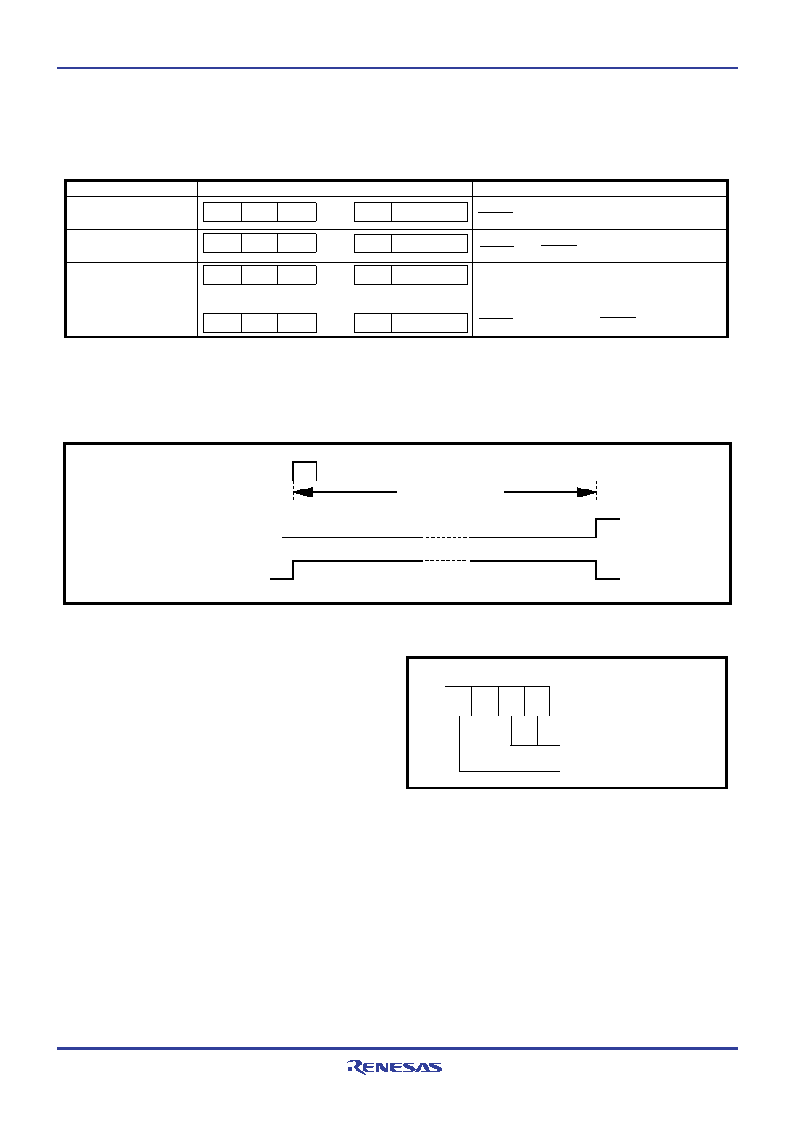
Table 13 Change of successive comparison register AD during A/D conversion
Comparison voltage (Vref) value
Change of successive comparison register AD
At starting conversion
±
1: 1st comparison result
3: 3rd comparison result
9: 9th comparison result
2: 2nd comparison result
8: 8th comparison result
A: 10th comparison result
1st comparison
2nd comparison
3rd comparison
After 10th comparison
completes
1
-----
0
1
2
0
1
3
0
8
0
9
0
A
A/D conversion result
VDD
2
VDD
2
VDD
2
VDD
2
VDD
4
VDD
4
VDD
8
VDD
1024
○○○
○
-------------
Fig. 30 Setting registers
A/D control register Q1
AIN1 pin selected
A/D conversion mode
0
001
(Bit 3)
(Bit 0)
(7) A/D conversion timing chart
Figure 29 shows the A/D conversion timing chart.
Fig. 29 A/D conversion timing chart
(8) How to use A/D conversion
How to use A/D conversion is explained using as example in which
the analog input from P21/AIN1 pin is A/D converted, and the high-
order 4 bits of the converted data are stored in address M(Z, X, Y)
= (0, 0, 0), the middle-order 4 bits in address M(Z, X, Y) = (0, 0, 1),
and the low-order 2 bits in address M(Z, X, Y) = (0, 0, 2) of RAM.
The A/D interrupt is not used in this example.
Select the AIN1 pin function and A/D conversion mode with the
register Q1 (refer to Figure 30).
Execute the ADST instruction and start A/D conversion.
Examine the state of ADF flag with the SNZAD instruction to de-
termine the end of A/D conversion.
Transfer the low-order 2 bits of converted data to the high-order
2 bits of register A (TALA instruction).
Transfer the contents of register A to M (Z, X, Y) = (0, 0, 2).
Transfer the high-order 8 bits of converted data to registers A
and B (TABAD instruction).
Transfer the contents of register A to M (Z, X, Y) = (0, 0, 1).
Transfer the contents of register B to register A, and then, store
into M(Z, X, Y) = (0, 0, 0).
ADST instruction
A/D conversion
completion flag (ADF)
62 machine cycles
DAC operation signal
相關(guān)PDF資料 |
PDF描述 |
|---|---|
| M34501M4-XXXFP | 4-BIT, MROM, MICROCONTROLLER, PDSO20 |
| M34501E4FP | 4-BIT, OTPROM, MICROCONTROLLER, PDSO20 |
| M34502M2-XXXFP | 4-BIT, MROM, MICROCONTROLLER, PDSO24 |
| M34502M4-XXXFP | 4-BIT, MROM, MICROCONTROLLER, PDSO24 |
| M34506M4-XXXFP | 4-BIT, MROM, MICROCONTROLLER, PDSO20 |
相關(guān)代理商/技術(shù)參數(shù) |
參數(shù)描述 |
|---|---|
| M34501M2 | 制造商:MITSUBISHI 制造商全稱(chēng):Mitsubishi Electric Semiconductor 功能描述:SINGLE-CHIP 4-BIT CMOS MICROCOMPUTER |
| M34501M2-XXXFP | 制造商:RENESAS 制造商全稱(chēng):Renesas Technology Corp 功能描述:SINGLE-CHIP 4-BIT CMOS MICROCOMPUTER |
| M34501M4 | 制造商:MITSUBISHI 制造商全稱(chēng):Mitsubishi Electric Semiconductor 功能描述:SINGLE-CHIP 4-BIT CMOS MICROCOMPUTER |
| M34501M4-XXXFP | 制造商:MITSUBISHI 制造商全稱(chēng):Mitsubishi Electric Semiconductor 功能描述:SINGLE-CHIP 4-BIT CMOS MICROCOMPUTER |
| M34502E4 | 制造商:RENESAS 制造商全稱(chēng):Renesas Technology Corp 功能描述:SINGLE-CHIP 4-BIT CMOS MICROCOMPUTER |
發(fā)布緊急采購(gòu),3分鐘左右您將得到回復(fù)。