- 您現(xiàn)在的位置:買賣IC網(wǎng) > PDF目錄69010 > M34238MK-XXXGP 4-BIT, MROM, 4 MHz, MICROCONTROLLER, PDSO20 PDF資料下載
參數(shù)資料
| 型號: | M34238MK-XXXGP |
| 元件分類: | 微控制器/微處理器 |
| 英文描述: | 4-BIT, MROM, 4 MHz, MICROCONTROLLER, PDSO20 |
| 封裝: | PLASTIC, SOP-20 |
| 文件頁數(shù): | 27/41頁 |
| 文件大小: | 243K |
| 代理商: | M34238MK-XXXGP |
第1頁第2頁第3頁第4頁第5頁第6頁第7頁第8頁第9頁第10頁第11頁第12頁第13頁第14頁第15頁第16頁第17頁第18頁第19頁第20頁第21頁第22頁第23頁第24頁第25頁第26頁當前第27頁第28頁第29頁第30頁第31頁第32頁第33頁第34頁第35頁第36頁第37頁第38頁第39頁第40頁第41頁
MITSUBISHI MICROCOMPUTERS
4238 Group
32
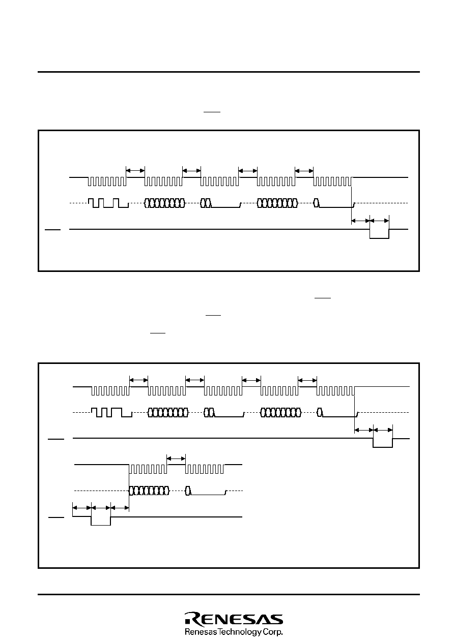
Program
Input command code 2516 in the first transfer. Proceed and input the
low-order 8 bits and high-order 8 bits of the address and the low-
order 8 bits and high-order 8 bits of program data, and pull the PGM
Fig.4 Timing at program verifying
Fig.3 Timing at programming
the program command is read and verified and stored into the in-
ternal data latch. When the PGM pin is released back to “H”, the
verify data that has been stored into the data latch is serially output
from the SDA pin.
Note. When outputting the verify data, the SDA pin is switched for output at the first falling of the serial clock. The SDA pin is placed in
the high-impedance state during the th(C–E) period after the last rising edge of the serial clock (at the 16th bit).
pin to “L”. When this is done, the program data is programmed to
the specified address.
Program verify
Input command code 3516 in the first transfer. Proceed and input the
low-order 8 bits and high-order 8 bits of the address and the low-
order 8 bits and high-order 8 bits of program data, and pull the PGM
pin to “L”. When this is done, the program data is programmed to
the specified address. Then, when the PGM pin is pulled to “L”
again after it is released back to “H”, the address programmed with
10 1001 00
A0
A7
Command code input
(2516)
Program address input (L) Program address input (H)
SCLK
SDA
PGM
Program
tCH
D0
D7
Program data input (L)
tCP
tWP
tCH
D8
Program data input (H)
tCH
00 00 00 0
tCH
A8 A9
0 0000 0
b0
b7
1 01 0 110 0
A0
A7
Command code input
(3516)
Program address input (L) Program address input (H)
SCLK
SDA
PGM
tCH
D0
D7
Program data input (L)
tCP
tWP
tCH
D8
Program data input (H)
tCH
00 0000 0
tCH
A8 A9
0000 0 0
tCR
tRC
SCLK
SDA
PGM
Verify
tWR
D0
D7
Verify data output (L)
D8
Verify data output (H)
tCH
0000 000
Program
b0
b7
PROM VERSION OF M34238MK-XXXGP
相關PDF資料 |
PDF描述 |
|---|---|
| M34250E2-XXXFP | 4-BIT, OTPROM, 4.4 MHz, MICROCONTROLLER, PDSO20 |
| M34250M2-XXXFP | 4-BIT, MROM, 4.4 MHz, MICROCONTROLLER, PDSO20 |
| M34250M2-XXXFP | 4-BIT, MROM, 4.4 MHz, MICROCONTROLLER, PDSO20 |
| M34280M1-XXXFP | 4-BIT, MROM, 4 MHz, MICROCONTROLLER, PDSO20 |
| M34280M1-XXXGP | 4-BIT, MROM, 4 MHz, MICROCONTROLLER, PDSO20 |
相關代理商/技術參數(shù) |
參數(shù)描述 |
|---|---|
| M3424 SL001 | 制造商:Alpha Wire Company 功能描述:CBL 6PR 24AWG SLT 1000' |
| M3424 SL002 | 制造商:Alpha Wire Company 功能描述:CBL 6PR 24AWG SLT 500' |
| M3424 SL005 | 制造商:Alpha Wire Company 功能描述:CBL 6PR 24AWG SLT 100' |
| M3424-0003 | 制造商:Bonitron 功能描述:OVERVOLTAGE BRAKING TRANSISTOR |
| M3424-SL002 | 制造商:Alpha Wire 功能描述: |
發(fā)布緊急采購,3分鐘左右您將得到回復。