- 您現(xiàn)在的位置:買賣IC網(wǎng) > PDF目錄67760 > M306H2MC-XXXFP 16-BIT, MROM, 10 MHz, MICROCONTROLLER, PQFP116 PDF資料下載
參數(shù)資料
| 型號: | M306H2MC-XXXFP |
| 元件分類: | 微控制器/微處理器 |
| 英文描述: | 16-BIT, MROM, 10 MHz, MICROCONTROLLER, PQFP116 |
| 封裝: | 20 X 20 MM, 0.65 MM PITCH, PLASTIC, LQFP-116 |
| 文件頁數(shù): | 5/212頁 |
| 文件大?。?/td> | 2877K |
| 代理商: | M306H2MC-XXXFP |
第1頁第2頁第3頁第4頁當(dāng)前第5頁第6頁第7頁第8頁第9頁第10頁第11頁第12頁第13頁第14頁第15頁第16頁第17頁第18頁第19頁第20頁第21頁第22頁第23頁第24頁第25頁第26頁第27頁第28頁第29頁第30頁第31頁第32頁第33頁第34頁第35頁第36頁第37頁第38頁第39頁第40頁第41頁第42頁第43頁第44頁第45頁第46頁第47頁第48頁第49頁第50頁第51頁第52頁第53頁第54頁第55頁第56頁第57頁第58頁第59頁第60頁第61頁第62頁第63頁第64頁第65頁第66頁第67頁第68頁第69頁第70頁第71頁第72頁第73頁第74頁第75頁第76頁第77頁第78頁第79頁第80頁第81頁第82頁第83頁第84頁第85頁第86頁第87頁第88頁第89頁第90頁第91頁第92頁第93頁第94頁第95頁第96頁第97頁第98頁第99頁第100頁第101頁第102頁第103頁第104頁第105頁第106頁第107頁第108頁第109頁第110頁第111頁第112頁第113頁第114頁第115頁第116頁第117頁第118頁第119頁第120頁第121頁第122頁第123頁第124頁第125頁第126頁第127頁第128頁第129頁第130頁第131頁第132頁第133頁第134頁第135頁第136頁第137頁第138頁第139頁第140頁第141頁第142頁第143頁第144頁第145頁第146頁第147頁第148頁第149頁第150頁第151頁第152頁第153頁第154頁第155頁第156頁第157頁第158頁第159頁第160頁第161頁第162頁第163頁第164頁第165頁第166頁第167頁第168頁第169頁第170頁第171頁第172頁第173頁第174頁第175頁第176頁第177頁第178頁第179頁第180頁第181頁第182頁第183頁第184頁第185頁第186頁第187頁第188頁第189頁第190頁第191頁第192頁第193頁第194頁第195頁第196頁第197頁第198頁第199頁第200頁第201頁第202頁第203頁第204頁第205頁第206頁第207頁第208頁第209頁第210頁第211頁第212頁
SINGLE-CHIP 16-BIT CMOS MICROCOMPUTER
with DATA ACQUISITION CONTROLLER
MITSUBISHI MICROCOMPUTERS
99
Rev. 1.0
M306H2MC-XXXFP
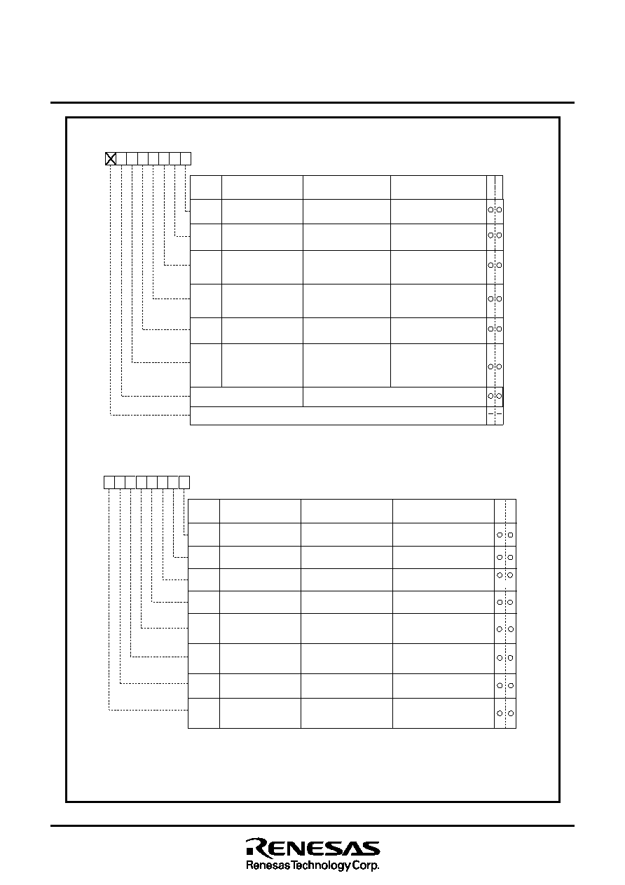
Note: When using multiple pins to output the transfer clock, the following requirements must be met:
UART1 internal/external clock select bit (bit 3 at address 03A816) = “0”.
UART transmit/receive control register 2
Symbol
Address
When reset
UCON
03B016
X00000002
b7
b6
b5
b4
b3
b2
b1
b0
Bit name
Bit
symbol
W
R
Function
(During UART mode)
Function
(During clock synchronous
serial I/O mode)
CLKMD0
CLKMD1
Reserved bit
UART0 transmit
interrupt cause select bit
UART0 continuous
receive mode enable bit
0 : Continuous receive
mode disabled
1 : Continuous receive
mode enable
UART1 continuous
receive mode enable bit
CLK/CLKS select bit 0
UART1 transmit
interrupt cause select bit
0 : Transmit buffer empty (Tl = 1)
1 : Transmission completed
(TXEPT = 1)
0 : Transmit buffer empty (Tl = 1)
(TXEPT = 1)
1 : Transmission completed
0 : Normal mode
(CLK output is CLK1 only)
1 : Transfer clock output
from multiple pins
function selected
0 : Continuous receive
mode disabled
1 : Continuous receive
mode enabled
Nothing is assigned.
In an attempt to write to this bit, write “0”. The value, if read, turns out to be indeterminate.
0 : Transmit buffer empty (Tl = 1)
1 : Transmission completed
(TXEPT = 1)
0 : Transmit buffer empty (Tl = 1)
1 : Transmission completed
(TXEPT = 1)
Must always be “0”
U0IRS
U1IRS
U0RRM
U1RRM
Invalid
CLK/CLKS select bit
1 (Note)
Valid when bit 5 = “1”
0 : Clock output to CLK1
1 : Clock output to CLKS1
UART2 special mode register
Symbol
Address
When reset
U2SMR
037716
0016
b7 b6 b5 b4 b3 b2 b1 b0
Bit name
Bit
symbol
Function
(During clock synchronous
serial I/O mode)
ABSCS
ACSE
SSS
I2C mode selection bit
Bus busy flag
0 : STOP condition detected
1 : START condition detected
SCLL sync output
enable bit
Bus collision detect
sampling
clock select bit
Arbitration lost detecting
flag control bit
0 : Normal mode
1 : I2C mode
0 : Update per bit
1 : Update per byte
IICM
ABC
BBS
LSYN
0 : Disabled
1 : Enabled
Transmit start condition
select bit
Auto clear function
select bit of transmit
enable bit
Must always be “0”
0
Must always be “0”
SDDS
SDA digital delay
selection bit
(Notes 2 and 3)
W
R
Function
(During UART mode)
0 : Ordinary
1 : Falling edge of RxD2
Must always be “0”
0 : Rising edge of transfer
clock
1 : Underflow signal of timer A0
0 : No auto clear function
1 : Auto clear at occurrence of
bus collision
Must always be “0”
0 : Analog delay output
selection
1 : Digital delay output selection
(Note 1)
Notes 1: Nothing but "0" may be written.
2: Do not write "1" except at I2C mode. Must always be “0” at normal mode.
Bit 7 to bit5 (DL2 to DL0 = SDA digital delay value setting bit) of UART2 special mode
register 3 (U2SMR3/address 037516) are initialized and become “000” when this bit is "0", analog
delay circuit is selected. Reading and writing U2SMR3 are enablewhen SDDS = "0".
3: Delaying ; Only analog delay value when analog delay is selected, and only digital delay value
when digital delay is selected.
Figure 2.11.8 UARTi I/O-related registers (5)
相關(guān)PDF資料 |
PDF描述 |
|---|---|
| M306H7MG-XXXFP | 16-BIT, MROM, 16 MHz, MICROCONTROLLER, PQFP100 |
| M306H7MC-XXXFP | 16-BIT, MROM, 16 MHz, MICROCONTROLLER, PQFP100 |
| M306NMFHTGP | 16-BIT, FLASH, 20 MHz, MICROCONTROLLER, PQFP128 |
| M306NMFJVGP | 16-BIT, FLASH, 20 MHz, MICROCONTROLLER, PQFP128 |
| M306NKFJVGP | 16-BIT, FLASH, 20 MHz, MICROCONTROLLER, PQFP100 |
相關(guān)代理商/技術(shù)參數(shù) |
參數(shù)描述 |
|---|---|
| M306H2T-RPD-E | 制造商:Renesas Electronics Corporation 功能描述:EMULATION POD, M16C6H GROUP (M306H2) - Bulk |
| M306H3FCFP | 制造商:RENESAS 制造商全稱:Renesas Technology Corp 功能描述:SINGLE-CHIP 16-BIT CMOS MICROCOMPUTER with DATA ACQUISITION CONTROLLER |
| M306H3FCFP#U0 | 制造商:Renesas Electronics Corporation 功能描述:MCU 16BIT R8C CISC 128KB FLASH 5V 116LQFP - Trays |
| M306H3MC-XXXFP | 制造商:RENESAS 制造商全稱:Renesas Technology Corp 功能描述:SINGLE-CHIP 16-BIT CMOS MICROCOMPUTER with DATA ACQUISITION CONTROLLER |
| M306H5FGFP | 制造商:RENESAS 制造商全稱:Renesas Technology Corp 功能描述:SNGLE-CHIP 16-BIT CMOS MICROCOMPUTER with DATA ACQUISITION CONTROLLER |
發(fā)布緊急采購,3分鐘左右您將得到回復(fù)。