- 您現(xiàn)在的位置:買賣IC網(wǎng) > PDF目錄69008 > M30220FCRP 16-BIT, FLASH, 10 MHz, MICROCONTROLLER, PQFP144 PDF資料下載
參數(shù)資料
| 型號(hào): | M30220FCRP |
| 元件分類: | 微控制器/微處理器 |
| 英文描述: | 16-BIT, FLASH, 10 MHz, MICROCONTROLLER, PQFP144 |
| 封裝: | 16 X 16 MM, 0.40 MM PITCH, PLASTIC, TQFP-144 |
| 文件頁數(shù): | 194/223頁 |
| 文件大小: | 3099K |
| 代理商: | M30220FCRP |
第1頁第2頁第3頁第4頁第5頁第6頁第7頁第8頁第9頁第10頁第11頁第12頁第13頁第14頁第15頁第16頁第17頁第18頁第19頁第20頁第21頁第22頁第23頁第24頁第25頁第26頁第27頁第28頁第29頁第30頁第31頁第32頁第33頁第34頁第35頁第36頁第37頁第38頁第39頁第40頁第41頁第42頁第43頁第44頁第45頁第46頁第47頁第48頁第49頁第50頁第51頁第52頁第53頁第54頁第55頁第56頁第57頁第58頁第59頁第60頁第61頁第62頁第63頁第64頁第65頁第66頁第67頁第68頁第69頁第70頁第71頁第72頁第73頁第74頁第75頁第76頁第77頁第78頁第79頁第80頁第81頁第82頁第83頁第84頁第85頁第86頁第87頁第88頁第89頁第90頁第91頁第92頁第93頁第94頁第95頁第96頁第97頁第98頁第99頁第100頁第101頁第102頁第103頁第104頁第105頁第106頁第107頁第108頁第109頁第110頁第111頁第112頁第113頁第114頁第115頁第116頁第117頁第118頁第119頁第120頁第121頁第122頁第123頁第124頁第125頁第126頁第127頁第128頁第129頁第130頁第131頁第132頁第133頁第134頁第135頁第136頁第137頁第138頁第139頁第140頁第141頁第142頁第143頁第144頁第145頁第146頁第147頁第148頁第149頁第150頁第151頁第152頁第153頁第154頁第155頁第156頁第157頁第158頁第159頁第160頁第161頁第162頁第163頁第164頁第165頁第166頁第167頁第168頁第169頁第170頁第171頁第172頁第173頁第174頁第175頁第176頁第177頁第178頁第179頁第180頁第181頁第182頁第183頁第184頁第185頁第186頁第187頁第188頁第189頁第190頁第191頁第192頁第193頁當(dāng)前第194頁第195頁第196頁第197頁第198頁第199頁第200頁第201頁第202頁第203頁第204頁第205頁第206頁第207頁第208頁第209頁第210頁第211頁第212頁第213頁第214頁第215頁第216頁第217頁第218頁第219頁第220頁第221頁第222頁第223頁
Timer A
Mitsubishi microcomputers
M30220 Group
SINGLE-CHIP 16-BIT CMOS MICROCOMPUTER
69
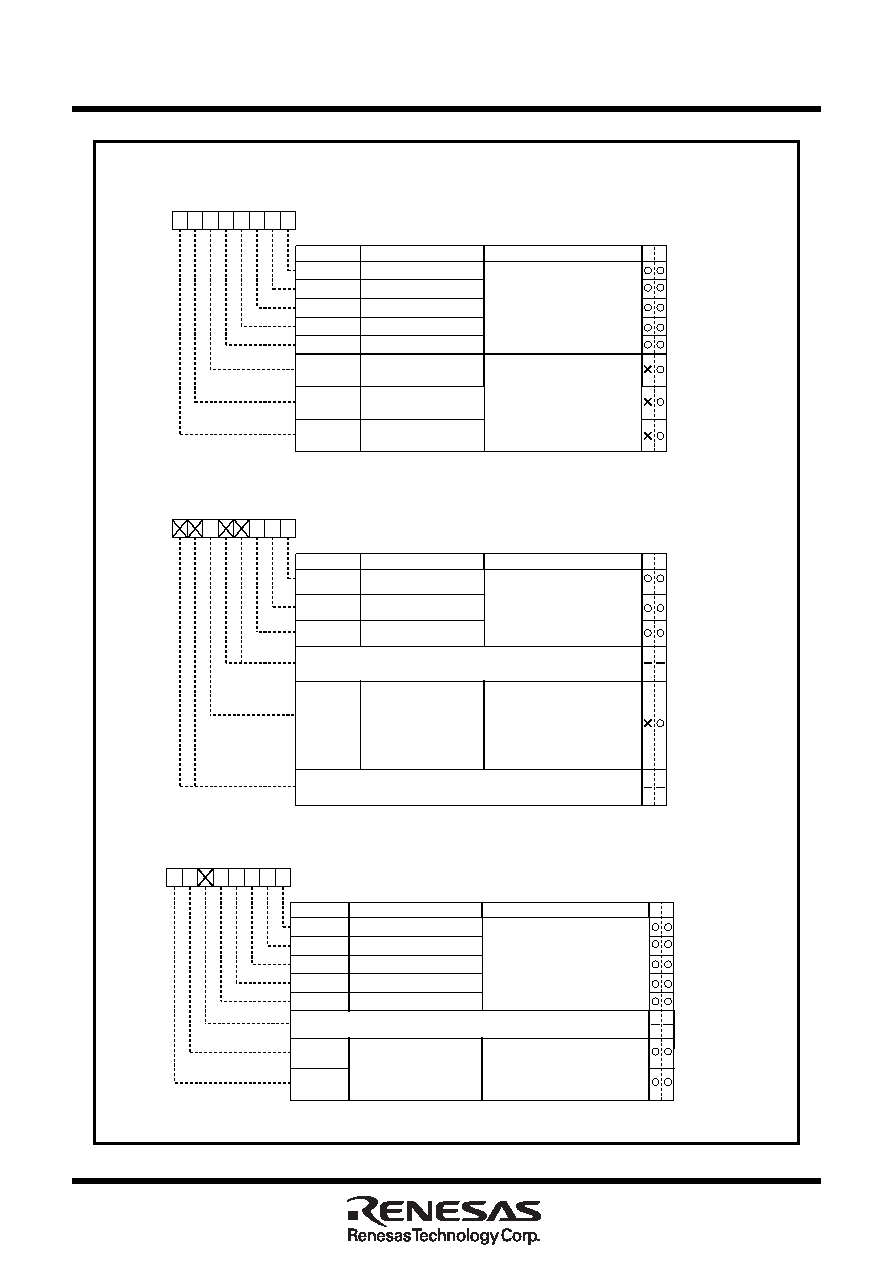
Figure 1.13.6. Timer A-related registers (3)
Timer A7 up/down flag
Timer A6 up/down flag
Timer A5 up/down flag
Timer A7 two-phase pulse
signal processing select bit
Symbol
Address
When reset
UDF1
034416
XX0XX0002
TA7P
Up/down flag 1 (Note)
Bit name
Function
Bit symbol
W
R
b7
b6
b5
b4
b3
b2
b1
b0
TA7UD
TA6UD
TA5UD
0 : Down count
1 : Up count
This specification becomes valid
when the up/down flag content is
selected for up/down switching
cause
0 : two-phase pulse signal
processing disabled
1 : two-phase pulse signal
processing enabled
When not using the two-phase
pulse signal processing function,
set the select bit to “0”
Nothing is assigned.
In an attempt to write to these bits, write “0”. The value, if read, turns out to be
indeterminate.
Nothing is assigned.
In an attempt to write to these bits, write “0”. The value, if read, turns out to be
indeterminate.
Timer A4 up/down flag
Timer A3 up/down flag
Timer A2 up/down flag
Timer A1 up/down flag
Timer A0 up/down flag
Timer A2 two-phase pulse
signal processing select bit
Timer A3 two-phase pulse
signal processing select bit
Timer A4 two-phase pulse
signal processing select bit
Symbol
Address
When reset
UDF0
038416
0016
TA4P
TA3P
TA2P
Up/down flag 0 (Note)
Bit name
Function
Bit symbol
W
R
b7
b6
b5
b4
b3
b2
b1
b0
TA4UD
TA3UD
TA2UD
TA1UD
TA0UD
0 : Down count
1 : Up count
This specification becomes valid
when the up/down flag content is
selected for up/down switching
cause
0 : two-phase pulse signal
processing disabled
1 : two-phase pulse signal
processing enabled
When not using the two-phase
pulse signal processing function,
set the select bit to “0”
TA1OS
TA2OS
TA0OS
One-shot start flag 0
Symbol
Address
When reset
ONSF0
038216
00X000002
Timer A0 one-shot start flag
Timer A1 one-shot start flag
Timer A2 one-shot start flag
Timer A3 one-shot start flag
Timer A4 one-shot start flag
TA3OS
TA4OS
Bit name
Function
Bit symbol
b7
b6
b5
b4
b3
b2
b1
b0
Nothing is assigned.
In an attempt to write to this bit, write “0”. The value, if read, turns out to be indeterminate.
TA0TGL
TA0TGH
0 0 : Input on TA0IN is selected (Note)
0 1 : TB2 overflow is selected
1 0 : TA4 overflow is selected
1 1 : TA1 overflow is selected
Timer A0 event/trigger
select bit
b7 b6
Note: Set the corresponding port direction register to “0”.
W
R
1 : Timer start
When read, the value is “0”
Note : Use MOV instruction to write to this register.
相關(guān)PDF資料 |
PDF描述 |
|---|---|
| M30220MA-XXXGP | 16-BIT, MROM, 10 MHz, MICROCONTROLLER, PQFP144 |
| M30220MA-XXXRP | 16-BIT, MROM, 10 MHz, MICROCONTROLLER, PQFP144 |
| M30220FCRP | 16-BIT, FLASH, 10 MHz, MICROCONTROLLER, PQFP144 |
| M30220FCGP | 16-BIT, FLASH, 10 MHz, MICROCONTROLLER, PQFP144 |
| M30220MA-XXXGP | 16-BIT, MROM, 10 MHz, MICROCONTROLLER, PQFP144 |
相關(guān)代理商/技術(shù)參數(shù) |
參數(shù)描述 |
|---|---|
| M30220M8-XXXGP | 制造商:RENESAS 制造商全稱:Renesas Technology Corp 功能描述:SINGLE-CHIP 16-BIT CMOS MICROCOMPUTER |
| M30220M8-XXXRP | 制造商:RENESAS 制造商全稱:Renesas Technology Corp 功能描述:SINGLE-CHIP 16-BIT CMOS MICROCOMPUTER |
| M30220MA | 制造商:MITSUBISHI 制造商全稱:Mitsubishi Electric Semiconductor 功能描述:SINGLE-CHIP 16-BIT CMOS MICROCOMPUTER |
| M30220MA-101GP | 制造商:MITSUBISHI 制造商全稱:Mitsubishi Electric Semiconductor 功能描述:SINGLE-CHIP 16-BIT CMOS MICROCOMPUTER |
| M30220MA-101RP | 制造商:MITSUBISHI 制造商全稱:Mitsubishi Electric Semiconductor 功能描述:SINGLE-CHIP 16-BIT CMOS MICROCOMPUTER |
發(fā)布緊急采購,3分鐘左右您將得到回復(fù)。