- 您現(xiàn)在的位置:買賣IC網(wǎng) > PDF目錄358997 > M27V102-90N1TR (意法半導(dǎo)體) 1 Mbit 64Kb x 16 Low Voltage UV EPROM and OTP EPROM PDF資料下載
參數(shù)資料
| 型號: | M27V102-90N1TR |
| 廠商: | 意法半導(dǎo)體 |
| 英文描述: | 1 Mbit 64Kb x 16 Low Voltage UV EPROM and OTP EPROM |
| 中文描述: | 1兆位64Kb的× 16低壓紫外線存儲器和OTP存儲器 |
| 文件頁數(shù): | 4/15頁 |
| 文件大?。?/td> | 116K |
| 代理商: | M27V102-90N1TR |

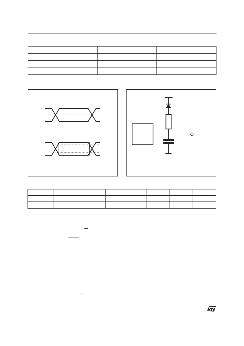
AI01822
3V
High Speed
0V
1.5V
2.4V
Standard
0.4V
2.0V
0.8V
Figure 3. AC TestingInput Output Waveform
AI01823B
1.3V
OUT
CL
CL= 30pF for High Speed
CL= 100pF for Standard
CLincludes JIG capacitance
3.3k
1N914
DEVICE
UNDER
TEST
Figure 4. AC Testing Load Circuit
High Speed
Standard
Input Rise and Fall Times
≤
10ns
≤
20ns
Input Pulse Voltages
0 to 3V
0.4V to 2.4V
Input and Output Timing Ref. Voltages
1.5V
0.8V and 2V
Table5. AC MeasurementConditions
Symbol
Parameter
Test Condition
Min
Max
Unit
C
IN
Input Capacitance
V
IN
= 0V
6
pF
C
OUT
Output Capacitance
V
OUT
= 0V
12
pF
Note:
1. Sampledonly, not 100% tested.
Table 6. Capacitance
(1)
(T
A
= 25
°
C, f = 1 MHz )
Forthe mostefficientuseof thesetwocontrollines,
E should be decoded and used as the primary
deviceselecting function,while G shouldbe made
a common connection to all devices in the array
and connected to the READ line from the system
controlbus. Thisensuresthatall deselectedmem-
ory devices are in their low power standby mode
and that the output pins are only active when data
is required from a particularmemory device.
SystemConsiderations
The power switching characteristics of Advanced
CMOS EPROMsrequire careful decouplingof the
devices. The supply current, I
CC
, has three seg-
ments that are of interestto the system designer:
the standby current level, the active current level,
and transient current peaks that are produced by
thefallingand risingedgesof E. Themagnitudeof
transientcurrentpeaksisdependentonthecapaci-
tive and inductive loading of the device at the
output.
The associated transient voltage peaks can be
suppressedby complying with the two line output
control and by properly selected decoupling ca-
pacitors. It is recommended that a 0.1
μ
F ceramic
capacitor be used on every device between V
CC
andV
SS
. Thisshouldbea highfrequencycapacitor
of low inherent inductance and should be placed
as close to the device as possible. In addition, a
4.7
μ
F bulk electrolytic capacitor should be used
betweenVcc and V
SS
for every eightdevices. The
bulk capacitor should be located near the power
supply connection point. The purpose of the bulk
capacitoris to overcome the voltage drop caused
by the inductiveeffectsof PCBtraces.
4/15
M27V102
相關(guān)PDF資料 |
PDF描述 |
|---|---|
| M27V102-90N6TR | 1 Mbit 64Kb x 16 Low Voltage UV EPROM and OTP EPROM |
| M27V160-150B1TR | 16 Mbit 2Mb x8 or 1Mb x16 Low Voltage UV EPROM and OTP EPROM |
| M27V160-150XF1TR | 16 Mbit 2Mb x8 or 1Mb x16 Low Voltage UV EPROM and OTP EPROM |
| M27V160-150XF6TR | 16 Mbit 2Mb x8 or 1Mb x16 Low Voltage UV EPROM and OTP EPROM |
| M27V160-200XM6TR | 16 Mbit 2Mb x8 or 1Mb x16 Low Voltage UV EPROM and OTP EPROM |
相關(guān)代理商/技術(shù)參數(shù) |
參數(shù)描述 |
|---|---|
| M27V102-90N6TR | 制造商:STMICROELECTRONICS 制造商全稱:STMicroelectronics 功能描述:1 Mbit 64Kb x 16 Low Voltage UV EPROM and OTP EPROM |
| M27V160 | 制造商:STMICROELECTRONICS 制造商全稱:STMicroelectronics 功能描述:16 Mbit (2Mb x8 or 1Mb x16) Low Voltage UV EPROM and OTP EPROM |
| M27V160_06 | 制造商:STMICROELECTRONICS 制造商全稱:STMicroelectronics 功能描述:16 Mbit (2Mb x8 or 1Mb x16) Low Voltage UV EPROM and OTP EPROM |
| M27V160-100B1 | 制造商:STMICROELECTRONICS 制造商全稱:STMicroelectronics 功能描述:16 Mbit (2Mb x8 or 1Mb x16) Low Voltage UV EPROM and OTP EPROM |
| M27V160-100B1TR | 制造商:STMICROELECTRONICS 制造商全稱:STMicroelectronics 功能描述:16 Mbit 2Mb x8 or 1Mb x16 Low Voltage UV EPROM and OTP EPROM |
發(fā)布緊急采購,3分鐘左右您將得到回復(fù)。