- 您現(xiàn)在的位置:買賣IC網(wǎng) > PDF目錄69008 > LX1684CDT (MICROSEMI CORP-ANALOG MIXED SIGNAL GROUP) 1 A SWITCHING CONTROLLER, 200 kHz SWITCHING FREQ-MAX, PDSO14 PDF資料下載
參數(shù)資料
| 型號: | LX1684CDT |
| 廠商: | MICROSEMI CORP-ANALOG MIXED SIGNAL GROUP |
| 元件分類: | 穩(wěn)壓器 |
| 英文描述: | 1 A SWITCHING CONTROLLER, 200 kHz SWITCHING FREQ-MAX, PDSO14 |
| 封裝: | PLASTIC, SOIC-14 |
| 文件頁數(shù): | 5/12頁 |
| 文件大?。?/td> | 292K |
| 代理商: | LX1684CDT |
Microsemi
Linfinity Microelectronics Division
11861 Western Avenue, Garden Grove, CA. 92841, 714-898-8121, Fax: 714-893-2570
Page 2
Copyright
2000
Rev. 1.0, 2001-09-19
WWW
.M
ic
ro
sem
i
.COM
LX1684
Voltage-Mode PWM Controller
PRODUCTION
L I N F IN IT Y
D I V I S I O N
ABSOLUT E M AXI M U M RA T
ABSOL UT E M AXI M U M RA T I NGS (NOTE 1 )
INGS (NOTE 1 )
Supply Voltage (VC1) ......................................................................................18V
Supply Voltage (VCC) ........................................................................................7V
Input Voltage (CSP Pin).................................................................................. 14V
Output Drive Peak Current Source (500ns).................................................... 1.0A
Output Drive Peak Current Sink (500ns)........................................................ 1.0A
Input Voltage (SS/ENABLE Pin)...........................................................-0.3 to 6V
Operating Junction Temperature ..................................................................150°C
Storage Temperature ...................................................................-65°C to +150°C
Lead Temperature (Soldering 10 Seconds) ..................................................300°C
Note: Exceeding these ratings could cause damage to the device. All voltages are with respect to
Ground. Currents are positive into, negative out of specified terminal.
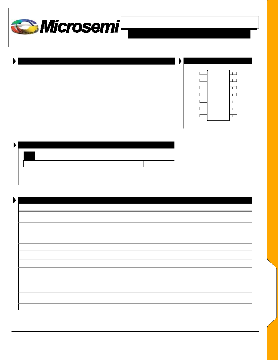
PACKAGE PIN OUT
1
2
4
3
14
13
11
12
14-PIN SOIC
(T op View)
5
6
10
7
9
8
TDRV
N/C
V
C1
N/C
CS
N/C
V
CC
FB
N/C
SS
VCSP
GND
PG ND
BDRV
THERMA L D A TA
D
PACKAGE
THERMAL RESISTANCE
-JUNCTION TO AMBIENT,
θθθθ
JA
165
°°°°C/W
Junction Temperature Calculation: TJ = TA + (PD x θJA).
The
θJA numbers are guidelines for the thermal performance of the device/pc-board
system. All of the above assume no ambient airflow.
FU N
F U N C TIONA L P I N D ESCRIP T
CTIONA L P I N D ESCRIP T
CTIONA L P I N D ESCRIP T ION
ION
PIN NAME
DESCRIPTION
VFB
Voltage Feedback. A 1.25V reference is connected to a resistor divider to set desired output voltage.
SS
Soft-Start And Hiccup Capacitor Pin. During start up the voltage of this pin controls the output voltage. An
internal 22k
resistor and the external capacitor set the time constant for soft-startup. Soft-start does not begin
until the supply voltage exceeds the UVLO threshold. When over-current occurs, this capacitor is used for timing
hiccup. The PWM can be disabled by pulling the SS pin below 0.3V
VCSP
Positive Over-Current Threshold Input
GND
Analog ground for SS, FB, CS and VCC.
PGND
MOSFET driver power ground
TDRV
Gate Drive For Upper MOSFET.
BDRV
Gate Drive For Lower MOSFET.
VC1
Separate Supply For MOSFET Gate Drives. Connect to gate drive voltage.
CS
Over-Current Set. Connect resistor between CS pin and the source of the upper MOSFET to set current-limit
point.
VCC
IC Supply Voltage (nominal 5V).
PP
AA
CC
KK
AA
GG
EE
DD
AA
TT
AA
相關(guān)PDF資料 |
PDF描述 |
|---|---|
| LX1689CPW-TR | FLUORESCENT LIGHT CONTROLLER, 500 kHz SWITCHING FREQ-MAX, PDSO20 |
| LX1689IPW-TR | FLUORESCENT LIGHT CONTROLLER, 500 kHz SWITCHING FREQ-MAX, PDSO20 |
| LX1691IPWTR | 0.1 A FLUORESCENT LIGHT CONTROLLER, 250 kHz SWITCHING FREQ-MAX, PDSO16 |
| LX1741CLM-TR | 0.145 A SWITCHING CONTROLLER, PDSO8 |
| LX1741CDU-TR | 0.145 A SWITCHING CONTROLLER, PDSO8 |
相關(guān)代理商/技術(shù)參數(shù) |
參數(shù)描述 |
|---|---|
| LX1684CD-TR | 制造商:MICROSEMI 制造商全稱:Microsemi Corporation 功能描述:Voltage-Mode PWM Controller |
| LX1686 | 制造商:MICROSEMI 制造商全稱:Microsemi Corporation 功能描述:Digital Dimming CCFL Controller IC |
| LX1686CPW | 功能描述:IC CTRLR CCFL BACKLIGHT 24TSSOP RoHS:是 類別:集成電路 (IC) >> PMIC - 照明,鎮(zhèn)流器控制器 系列:- 產(chǎn)品培訓(xùn)模塊:Lead (SnPb) Finish for COTS Obsolescence Mitigation Program 標準包裝:2,500 系列:- 類型:CCFL 控制器 頻率:40 ~ 80 kHz 電流 - 電源:5mA 電流 - 輸出:- 電源電壓:4.5 V ~ 5.5 V 工作溫度:-40°C ~ 85°C 封裝/外殼:16-SOIC(0.154",3.90mm 寬) 供應(yīng)商設(shè)備封裝:16-SOIC 包裝:帶卷 (TR) 其它名稱:90-3991V+V01 |
| LX1686CPWT | 制造商:未知廠家 制造商全稱:未知廠家 功能描述:Ballast/Backlight Controller/Driver |
| LX1686CPW-TR | 制造商:Microsemi Corporation 功能描述:CCFL Controller 3.3V/5V 24-Pin TSSOP T/R |
發(fā)布緊急采購,3分鐘左右您將得到回復(fù)。