- 您現在的位置:買賣IC網 > PDF目錄39437 > LV24030LP (SANYO SEMICONDUCTOR CO LTD) AUDIO TUNER, QCC24 PDF資料下載
參數資料
| 型號: | LV24030LP |
| 廠商: | SANYO SEMICONDUCTOR CO LTD |
| 元件分類: | 調諧器 |
| 英文描述: | AUDIO TUNER, QCC24 |
| 封裝: | 4 X 4 MM, 0.80 MM HEIGHT, VQLP-24 |
| 文件頁數: | 6/14頁 |
| 文件大小: | 171K |
| 代理商: | LV24030LP |
LV24030LP
No.A1003-14/14
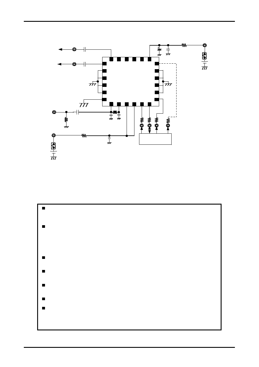
Application Circuit
Note1: Vale of Extenal Component is just reference. Please set most sutable value under Acutual_ operation.
Note2: Please take Consideration of most suitable_value, as for antenna application
Note3: We recomend to put R1,R2,R3,R4 for interface between MPU and IC.
Note4: Please put Capacitor Between VDD and GND also, put Capacitor Between VCC and GND as shown on
application.
Note5: As for AFC pin (16 pin), usually it is recommended not to connect anything. AFC can be operated more
smoothly by putting capacitor between 16 pin and GND.
PS
This catalog provides information as of January, 2008. Specifications and information herein are subject
to change without notice.
SANYO Semiconductor Co.,Ltd. assumes no responsibility for equipment failures that result from using
products at values that exceed, even momentarily, rated values (such as maximum ratings, operating condition
ranges, or other parameters) listed in products specifications of any and all SANYO Semiconductor Co.,Ltd.
products described or contained herein.
SANYO Semiconductor Co.,Ltd. strives to supply high-quality high-reliability products, however, any and all
semiconductor products fail or malfunction with some probability. It is possible that these probabilistic failures or
malfunction could give rise to accidents or events that could endanger human lives, trouble that could give rise
to smoke or fire, or accidents that could cause damage to other property. When designing equipment, adopt
safety measures so that these kinds of accidents or events cannot occur. Such measures include but are not
limited to protective circuits and error prevention circuits for safe design, redundant design, and structural
design.
Upon using the technical information or products described herein, neither warranty nor license shall be granted
with regard to intellectual property rights or any other rights of SANYO Semiconductor Co.,Ltd. or any third
party. SANYO Semiconductor Co.,Ltd. shall not be liable for any claim or suits with regard to a third party's
intellectual property rights which has resulted from the use of the technical information and products mentioned
above.
Information (including circuit diagrams and circuit parameters) herein is for example only; it is not guaranteed
for volume production.
Any and all information described or contained herein are subject to change without notice due to
product/technology improvement, etc. When designing equipment, refer to the "Delivery Specification" for the
SANYO Semiconductor Co.,Ltd. product that you intend to use.
In the event that any or all SANYO Semiconductor Co.,Ltd. products described or contained herein are
controlled under any of applicable local export control laws and regulations, such products may require the
export license from the authorities concerned in accordance with the above law.
No part of this publication may be reproduced or transmitted in any form or by any means, electronic or
mechanical, including photocopying and recording, or any information storage or retrieval system, or otherwise,
without the prior written consent of SANYO Semiconductor Co.,Ltd.
1
Line_out_L
Line_out_R
13
GND
47pF
100 to 1000pF
4.7
μH
MPU
FM_ANT
Package
GND
Package
GND
0.1
μF
1.0
μF
External_CLK_IN
VCC
Voltage
source
22
μF 0.1μF
SW
VDD
Voltage
source
SW
0.1
μF
V
CC
NR_W
V
IO
V
DD
CLO
C
K
DA
T
A
CLOC
K
DAT
A
NR
_W
External_
CLK_
IN
R1
R2
R3
200
Ω
to
1
kΩ
Not necessary
when the DC cut capacity
is on the receive side
2.2
μH or R:12Ω
Changeover of resistor possible
depending on the state of power
supply
27pF
120nH
Winding type
R4
4.7
μH or R:4.7Ω
Changeover of resistor possible
depending on the state of power
supply
相關PDF資料 |
PDF描述 |
|---|---|
| LV24030LP | AUDIO TUNER, QCC24 |
| LV24230LP-A | 1-BAND, AUDIO TUNER, QCC24 |
| LV24230LP-A | 1-BAND, AUDIO TUNER, QCC24 |
| LV4985VH | 1.2 W, 2 CHANNEL, AUDIO AMPLIFIER, PDSO14 |
| LV4985VH | 1.2 W, 2 CHANNEL, AUDIO AMPLIFIER, PDSO14 |
相關代理商/技術參數 |
參數描述 |
|---|---|
| LV24100LP | 制造商:SANYO 制造商全稱:Sanyo Semicon Device 功能描述:Bi-CMOS IC FM and AM Tuner IC for Small Portable Equipment |
| LV24100LP-TLM-E | 功能描述:調諧器 RoHS:否 制造商:NXP Semiconductors 功能: 噪聲系數: 工作電源電壓: 最小工作溫度: 最大工作溫度: |
| LV24230LP | 制造商:SANYO 制造商全稱:Sanyo Semicon Device 功能描述:Bi-CMOS LSI Compact Portable Equipment 1-Chip FM Tuner IC |
| LV24230LP-A | 制造商:SANYO 制造商全稱:Sanyo Semicon Device 功能描述:Compact Portable Equipment1-Chip FM Tuner IC |
| LV24230LP-A-TLM-E | 制造商:Sony Semiconductor Solutions Division 功能描述: |
發(fā)布緊急采購,3分鐘左右您將得到回復。