- 您現(xiàn)在的位置:買賣IC網(wǎng) > PDF目錄369855 > LTI969CMS Voltage-Feedback Operational Amplifier PDF資料下載
參數(shù)資料
| 型號: | LTI969CMS |
| 英文描述: | Voltage-Feedback Operational Amplifier |
| 中文描述: | 電壓反饋運算放大器 |
| 文件頁數(shù): | 13/20頁 |
| 文件大小: | 285K |
| 代理商: | LTI969CMS |
13
LT1969
network is bootstrapped. This network can also be placed
between the inverting input and an AC ground.
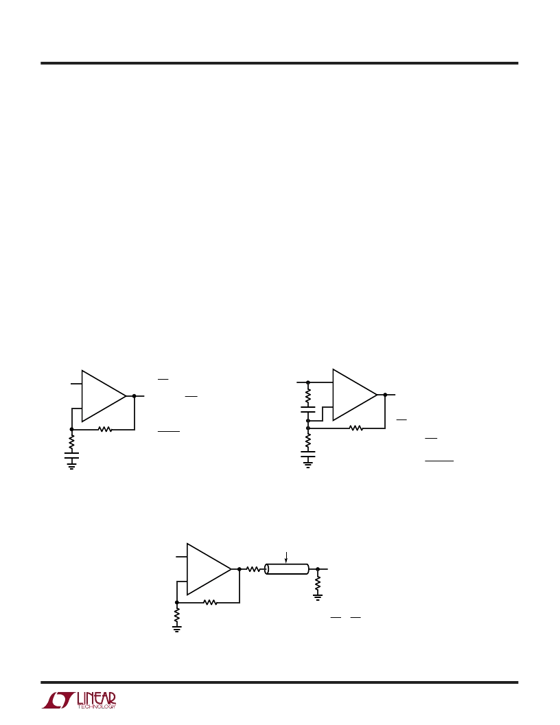
Another compensation scheme for noninverting circuits is
shown in Figure 4. The circuit is unity gain at low frequency
and a gain of 1 + R
F
/R
G
at high frequency. The DC output
offset is reduced by a factor of ten. The techniques of
Figures 3 and 4 can be combined as shown in Figure 5. The
gain is unity at low frequencies, 1 + R
F
/R
G
at mid-band and
for stability, a gain of 10 or greater at high frequencies.
Output Loading
The LT1969 output stage is very wide bandwidth and able
to source and sink large currents. Reactive loading, even
isolated with a back-termination resistor, can cause ring-
ing at frequencies of hundreds of MHz. For this reason, any
design should be evaluated over a wide range of output
conditions. To reduce the effects of reactive loading, an
optional snubber network consisting of a series RC across
the load can provide a resistive load at high frequency.
Another option is to filter the drive to the load. If a back-
termination resistor is used, a capacitor to ground at the
load can eliminate ringing.
Line Driving Back-Termination
The standard method of cable or line back-termination is
shown in Figure 6. The cable/line is terminated in its
characteristic impedance (50
, 75
, 100
, 135
, etc.).
A back-termination resistor also equal to to the
chararacteristic impedance should be used for maximum
pulse fidelity of outgoing signals, and to terminate the line
for incoming signals in a full-duplex application. There are
three main drawbacks to this approach. First, the power
dissipated in the load and back-termination resistors is
equal so half of the power delivered by the amplifier is
Figure 5. Combination Compensation
R
C
V
o
V
i
C
C
+
–
1969 F05
R
F
R
G
C
BIG
R
F
R
G
= 1 AT LOW FREQUENCIES
= 1 +
AT MEDIUM FREQUENCIES
R
F
(R
C
|| R
G
)
= 1 +
AT HIGH FREQUENCIES
V
o
V
i
Figure 4. Alternate Noninverting Compensation
+
–
1969 F04
R
F
R
G
V
i
V
O
C
C
< 15MHz
1
2
π
R
G
C
C
R
G
≤
R
F
/9
= 1 (LOW FREQUENCIES)
(HIGH FREQUENCIES)
V
o
V
i
= 1 +
R
F
R
G
Figure 6. Standard Cable/Line Back-Termination
+
–
1969 F06
R
F
R
BT
CABLE OR LINE WITH
CHARACTERISTIC IMPEDANCE R
L
R
G
V
O
V
i
R
L
(1 + R
F
/R
G
)
=
V
o
V
i
1
2
R
BT
= R
L
APPLICATIOU
W
U
U
相關PDF資料 |
PDF描述 |
|---|---|
| LTJ811G | Optoelectronic |
| LTJ811HR | Optoelectronic |
| LTJ811Y | Optoelectronic |
| LTK4N25 | Optoelectronic |
| LTK4N25V | Optoelectronic |
相關代理商/技術參數(shù) |
參數(shù)描述 |
|---|---|
| LTIGAB51-6S-BL-RC-MBL-XSW1 | 制造商:Carling Technologies 功能描述:LTIG, H, & L-SERIES RKR SW - Bulk |
| LTIGAB51-6S-WH-AM-NBL-XHA1 | 制造商:Carling Technologies 功能描述:LTIG, H, & L-SERIES RKR SW - Bulk |
| LTIGAB51-6S-WH-RC-WBLXTR5 | 制造商:Carling Technologies 功能描述:LTIG, H, & L-SERIES RKR SW - Bulk |
| LTIGAB53-6S-BL-RC-XWA1 | 制造商:Carling Technologies 功能描述:LTIG, H, & L-SERIES RKR SW - Bulk |
| LTIGAB56-7S-WH-RC-AXAC4 | 制造商:Carling Technologies 功能描述:LTIG, H, & L-SERIES RKR SW - Bulk |
發(fā)布緊急采購,3分鐘左右您將得到回復。