- 您現(xiàn)在的位置:買賣IC網(wǎng) > PDF目錄377783 > LTC693I (Linear Technology Corporation) Microprocessor Supervisory Circuits PDF資料下載
參數(shù)資料
| 型號: | LTC693I |
| 廠商: | Linear Technology Corporation |
| 英文描述: | Microprocessor Supervisory Circuits |
| 中文描述: | 微處理器監(jiān)控電路 |
| 文件頁數(shù): | 4/16頁 |
| 文件大小: | 308K |
| 代理商: | LTC693I |
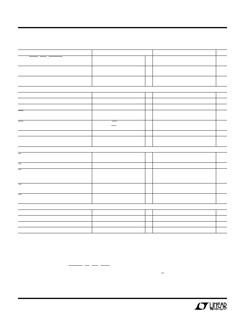
4
LTC692/LTC693
The
G
denotes specifications which apply over the full operating
temperature range.
Note 1:
Absolute maximum ratings are those values beyond which the life
of the device may be impaired.
Note 2:
All voltage values are with respect to GND.
Note 3:
For military temperature range, consult the factory.
Note 4:
The output pins of BATT ON, LOW LINE, PFO, WDO, RESET and
RESET have weak internal pull-ups of typically 3
μ
A. However, external
pull-up resistors may be used when higher speed is required.
V
CC
= Full Operating Range, V
BATT
= 2.8V, T
A
= 25
°
C, unless otherwise noted.
ELECTRICAL C
HARA TERISTICS
Note 5:
The LTC692/LTC693 have minimum reset active times of 140ms
(200ms typically). The reset active time of the LTC693 can be adjusted
(see Table 2 in Applications Information Section).
Note 6:
The external clock feeding into the circuit passes through the
oscillator before clocking the watchdog timer (See BLOCK DIAGRAM).
Variation in the time-out period is caused by phase errors which occur
when the oscillator divides the external clock by 64. The resulting variation
in the time-out period is 64 clocks plus one clock of jitter.
Note 7:
The input pins of CE IN, OSC IN and OSC SEL have weak internal
pull-ups which pull to the supply when the input pins are floating.
PARAMETER
RESET, RESET, WDO, LOW LINE
Output Short-Circuit Current (Note 4)
WDI Input Threshold
CONDITONS
Output Source Current
Output Sink Current
Logic Low
Logic High
WDI = V
OUT
WDI = 0V
MIN
1
TYP
3
25
MAX
25
UNITS
μ
A
mA
0.8
V
V
3.5
WDI Input Current
G
G
4
50
μ
A
μ
A
–50
–8
Power Fail Detector
PFI Input Threshold
PFI Input Threshold PSRR
PFI Input Current
PFO Output Voltage (Note 4)
V
CC
= 5V
G
1.25
1.3
0.3
±
0.01
1.35
V
mV/V
±
25
0.4
nA
V
V
μ
A
mA
μ
s
μ
s
μ
s
I
SINK
= 3.2mA
I
SOURCE
= 1
μ
A
PFI = HIGH, PFO = 0V
PFI = LOW, PFO = V
OUT
V
IN
= –20mV, V
OD
= 15mV
V
IN
= 20mV, V
OD
= 15mV
with 10k
Pull-Up
3.5
1
PFO Short Circuit Source Current
(Note 4)
PFI Comparator Response Time (falling)
PFI Comparator Response Time (rising)
(Note 4)
Chip Enable Gating
CE IN Threshold
3
25
2
40
8
25
V
IL
V
IH
0.8
V
V
2.0
CE IN Pullup Current (Note 7)
CE OUT Output Voltage
3
μ
A
V
V
V
ns
ns
mA
mA
I
SINK
= 3.2mA
I
SOURCE
= 3.0mA
I
SOURCE
= 1
μ
A, V
CC
= 0V
V
CC
= 5V, C
L
= 20pF
0.4
V
OUT
– 1.50
V
OUT
– 0.05
CE Propagation Delay
20
20
30
35
35
45
G
CE OUT Output Short Circuit Current
Output Source Current
Output Sink Current
Oscillator
OSC IN Input Current (Note 7)
OSC SEL Input Pull-Up Current (Note 7)
OSC IN Frequency Range
OSC IN Frequency with External Capacitor
±
2
5
μ
A
μ
A
kHz
kHz
OSC SEL = 0V
OSC SEL = 0V, C
OSC
= 47pF
G
0
250
4
相關(guān)PDF資料 |
PDF描述 |
|---|---|
| LTC692 | Microprocessor Supervisory Circuits(μP監(jiān)控電路) |
| LTC693 | Microprocessor Supervisory Circuits(μP監(jiān)控電路) |
| LTC694-3.3 | 3.3V Microprocessor Supervisory Circuits(3.3VμP監(jiān)控電路) |
| LTC695CSW-3.3 | 3.3V Microprocessor Supervisory Circuits |
| LTC695 | Microprocessor Supervisory Circuits |
相關(guān)代理商/技術(shù)參數(shù) |
參數(shù)描述 |
|---|---|
| LTC693IN | 制造商:LINER 制造商全稱:Linear Technology 功能描述:Microprocessor Supervisory Circuits |
| LTC693IS | 制造商:LINER 制造商全稱:Linear Technology 功能描述:Microprocessor Supervisory Circuits |
| LTC694 | 制造商:LINER 制造商全稱:Linear Technology 功能描述:Microprocessor Supervisory Circuits |
| LTC6943 | 制造商:LINER 制造商全稱:Linear Technology 功能描述:Micropower, Dual Precision Instrumentation Switched Capacitor Building Block |
| LTC694-3.3 | 制造商:LINER 制造商全稱:Linear Technology 功能描述:Low Voltage Supervisorwith 27 Selectable Thresholds and Watchdog Timer |
發(fā)布緊急采購,3分鐘左右您將得到回復(fù)。