- 您現(xiàn)在的位置:買賣IC網(wǎng) > PDF目錄377783 > LTC693I (Linear Technology Corporation) Microprocessor Supervisory Circuits PDF資料下載
參數(shù)資料
| 型號(hào): | LTC693I |
| 廠商: | Linear Technology Corporation |
| 英文描述: | Microprocessor Supervisory Circuits |
| 中文描述: | 微處理器監(jiān)控電路 |
| 文件頁(yè)數(shù): | 11/16頁(yè) |
| 文件大小: | 308K |
| 代理商: | LTC693I |
第1頁(yè)第2頁(yè)第3頁(yè)第4頁(yè)第5頁(yè)第6頁(yè)第7頁(yè)第8頁(yè)第9頁(yè)第10頁(yè)當(dāng)前第11頁(yè)第12頁(yè)第13頁(yè)第14頁(yè)第15頁(yè)第16頁(yè)
11
LTC692/LTC693
Power Fail Warning
The LTC692/LTC693 generate a Power Failure Output
(PFO) for early warning of failure in the microprocessor's
power supply. This is accomplished by comparing the
Power Failure Input (PFI) with an internal 1.3V reference.
PFO goes low when the voltage at the PFI pin is less than
1.3V. Typically PFI is driven by an external voltage divider
(R1 and R2 in Figures 8 and 9) which senses either an
unregulated DC input or a regulated 5V output. The voltage
divider ratio can be chosen such that the voltage at the PFI
pin falls below 1.3V, several milliseconds before the 5V
supply falls below the maximum reset voltage threshold of
4.50V. PFO is normally used to interrupt the microproces-
sor to execute shutdown procedure between PFO and
RESET or RESET.
The power fail comparator, C3, does not have hysteresis.
Hysteresis can be added however, by connecting a resis-
tor between the PFO output and the noninverting PFI input
pin as shown in Figures 8 and 9. The upper and lower trip
points in the comparator are established as follows:
When PFO output is low, R3 sinks current from the
summing junction at the PFI pin.
When PFO output is high, the series combination of R3 and
R4 source current into the PFI summing junction.
Example 1:
The circuit in Figure 8 demonstrates the use of
the power fail comparator to monitor the unregulated
power supply input. Assuming the the rate of decay of the
supply input V
IN
is 100mV/ms and the total time to execute
a shutdown procedure is 8ms. Also, the noise of V
IN
is
200mV. With these assumptions in mind, we can reason-
ably set V
L
= 7.25V which is 1.25V greater than the sum of
maximum reset voltage threshold and the dropout voltage
of LT1086-5 (4.5V + 1.5V) and V
HYSTERESIS
= 850mV.
U
S
A
O
PPLICATI
U
U
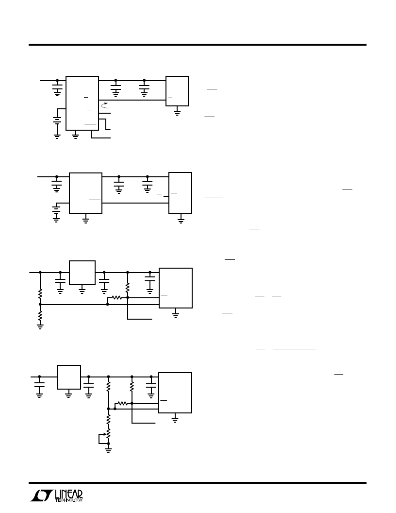
Figure 6. A Typical Nonvolatile CMOS RAM Application
5V
3V
0.1
μ
F
10
μ
F
V
BATT
V
CC
LTC693
V
OUT
GND
LTC692/3 F06
V
CC
RESET
CE IN
RESET
CE OUT
0.1
μ
F
TO
μ
P
FROM DECODER
CS
20ns PROPAGATION DELAY
62512
RAM
+
GND
Figure 7. Write Protect for RAM with the LTC692
5V
3V
0.1
μ
F
10
μ
F
V
BATT
V
CC
LTC692
V
OUT
GND
LTC692/3 F07
V
CC
RESET
0.1
μ
F
CS
62128
RAM
CS1
CS2
GND
+
V =1.3V 1+R1
R2
R1
R3
+
V
1.3V 1
R2–(5V–1.3V)R1
1.3V(R3
R4)
L
=
+
Assuming R4
R3,V
5VR1
R3
HYSTERESIS
<<
=
10
μ
F
10
μ
F
V
IN
V
OUT
ADJ
LTC692/3 F09
0.1
μ
F
TO
μ
P
LT1086-5
V
IN
≥
6.5V
+
R4
10k
R3
2.7M
+
R1
27k
R2
8.2k
5V
R5
3.3k
V
CC
GND
PFO
PFI
LTC692
LTC693
Figure 9. Monitoring RegulatedDC Supply
with the LTC692/LTC693 Power Fail Comparator
10
μ
F
100
μ
F
R3
300k
V
IN
V
OUT
ADJ
LTC692/3 F08
V
CC
0.1
μ
F
R4
10k
TO
μ
P
PFO
PFI
GND
LT1086-5
V
IN
≥
7.5V
LTC
LTC693
R1
51k
R2
10k
+
+
5V
Figure 8. Monitoring UnregulatedDC Supply with the
LTC692/LTC693 Power Fail Comparator
相關(guān)PDF資料 |
PDF描述 |
|---|---|
| LTC692 | Microprocessor Supervisory Circuits(μP監(jiān)控電路) |
| LTC693 | Microprocessor Supervisory Circuits(μP監(jiān)控電路) |
| LTC694-3.3 | 3.3V Microprocessor Supervisory Circuits(3.3VμP監(jiān)控電路) |
| LTC695CSW-3.3 | 3.3V Microprocessor Supervisory Circuits |
| LTC695 | Microprocessor Supervisory Circuits |
相關(guān)代理商/技術(shù)參數(shù) |
參數(shù)描述 |
|---|---|
| LTC693IN | 制造商:LINER 制造商全稱:Linear Technology 功能描述:Microprocessor Supervisory Circuits |
| LTC693IS | 制造商:LINER 制造商全稱:Linear Technology 功能描述:Microprocessor Supervisory Circuits |
| LTC694 | 制造商:LINER 制造商全稱:Linear Technology 功能描述:Microprocessor Supervisory Circuits |
| LTC6943 | 制造商:LINER 制造商全稱:Linear Technology 功能描述:Micropower, Dual Precision Instrumentation Switched Capacitor Building Block |
| LTC694-3.3 | 制造商:LINER 制造商全稱:Linear Technology 功能描述:Low Voltage Supervisorwith 27 Selectable Thresholds and Watchdog Timer |
發(fā)布緊急采購(gòu),3分鐘左右您將得到回復(fù)。