- 您現(xiàn)在的位置:買賣IC網(wǎng) > PDF目錄39410 > LTC2145IUP-14#PBF (LINEAR TECHNOLOGY CORP) 2-CH 14-BIT PROPRIETARY METHOD ADC, PARALLEL ACCESS, PQCC64 PDF資料下載
參數(shù)資料
| 型號(hào): | LTC2145IUP-14#PBF |
| 廠商: | LINEAR TECHNOLOGY CORP |
| 元件分類: | ADC |
| 英文描述: | 2-CH 14-BIT PROPRIETARY METHOD ADC, PARALLEL ACCESS, PQCC64 |
| 封裝: | 9 X 9 MM, LEAD FREE, PLASTIC, MO-220WNJR-5, QFN-64 |
| 文件頁數(shù): | 17/36頁 |
| 文件大小: | 827K |
| 代理商: | LTC2145IUP-14#PBF |
第1頁第2頁第3頁第4頁第5頁第6頁第7頁第8頁第9頁第10頁第11頁第12頁第13頁第14頁第15頁第16頁當(dāng)前第17頁第18頁第19頁第20頁第21頁第22頁第23頁第24頁第25頁第26頁第27頁第28頁第29頁第30頁第31頁第32頁第33頁第34頁第35頁第36頁
LTC2145-14/
LTC2144-14/LTC2143-14
24
21454314f
applicaTions inForMaTion
Phase Shifting the Output Clock
In full rate CMOS mode the data output bits normally
change at the same time as the falling edge of CLKOUT+,
so the rising edge of CLKOUT+ can be used to latch the
output data. In double data rate CMOS and LVDS modes
the data output bits normally change at the same time as
the falling and rising edges of CLKOUT+. To allow adequate
set-up and hold time when latching the data, the CLKOUT+
signal may need to be phase shifted relative to the data
output bits. Most FPGAs have this feature; this is generally
the best place to adjust the timing.
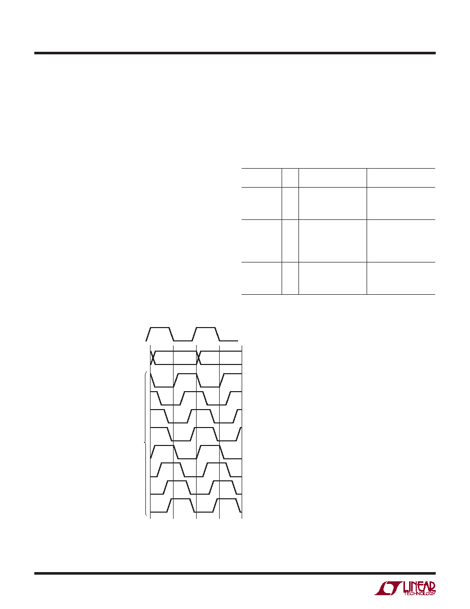
TheLTC2145-14/LTC2144-14/LTC2143-14canalsophase
shift the CLKOUT+/CLKOUT– signals by serially program-
ming mode control register A2. The output clock can be
shifted by 0°, 45°, 90°, or 135°. To use the phase shift-
ing feature the clock duty cycle stabilizer must be turned
on. Another control register bit can invert the polarity of
CLKOUT+ and CLKOUT–, independently of the phase shift.
Thecombinationofthesetwofeaturesenablesphaseshifts
of 45° up to 315° (Figure 14).
DATA FORMAT
Table 1 shows the relationship between the analog input
voltage, the digital data output bits and the overflow bit.
By default the output data format is offset binary. The 2’s
complement format can be selected by serially program-
ming mode control register A4.
Table 1. Output Codes vs Input Voltage
AIN+ – AIN–
(2V Range)
OF
D13-D0
(OFFSET BINARY)
D13-D0
(2’s COMPLEMENT)
>1.000000V
+0.999878V
+0.999756V
1
0
11 1111 1111 1111
11 1111 1111 1110
01 1111 1111 1111
01 1111 1111 1110
+0.000122V
+0.000000V
–0.000122V
–0.000244V
0
10 0000 0000 0001
10 0000 0000 0000
01 1111 1111 1111
01 1111 1111 1110
00 0000 0000 0001
00 0000 0000 0000
11 1111 1111 1111
11 1111 1111 1110
–0.999878V
–1.000000V
≤–1.000000V
0
1
00 0000 0000 0001
00 0000 0000 0000
10 0000 0000 0001
10 0000 0000 0000
CLKOUT+
D0-D13, OF
PHASE
SHIFT
0°
45°
90°
135°
180°
225°
270°
315°
CLKINV
0
1
CLKPHASE1
MODE CONTROL BITS
0
1
0
1
CLKPHASE0
0
1
0
1
0
1
0
1
21454314 F14
ENC+
Figure 14. Phase Shifting CLKOUT
相關(guān)PDF資料 |
PDF描述 |
|---|---|
| LTC2143CUP-14#PBF | 2-CH 14-BIT PROPRIETARY METHOD ADC, PARALLEL ACCESS, PQCC64 |
| LTC2144CUP-14#PBF | 2-CH 14-BIT PROPRIETARY METHOD ADC, PARALLEL ACCESS, PQCC64 |
| LTC2145CUP-14#TRPBF | 2-CH 14-BIT PROPRIETARY METHOD ADC, PARALLEL ACCESS, PQCC64 |
| LTC2145CUP-12#PBF | 2-CH 12-BIT PROPRIETARY METHOD ADC, PARALLEL ACCESS, PQCC64 |
| LTC2145IUP-12#TRPBF | 2-CH 12-BIT PROPRIETARY METHOD ADC, PARALLEL ACCESS, PQCC64 |
相關(guān)代理商/技術(shù)參數(shù) |
參數(shù)描述 |
|---|---|
| LTC2150-14 | 制造商:LINER 制造商全稱:Linear Technology 功能描述:300MHz Digital Predistortion Receiver |
| LTC2150CUJ-12#PBF | 制造商:Linear Technology 功能描述:IC ADC 12BIT 170MSPS 40QFN 制造商:Linear Technology 功能描述:ADC 12BIT 170MSPS SPI QFN-40 制造商:Linear Technology 功能描述:ADC, 12BIT, 170MSPS, SPI, QFN-40 制造商:Linear Technology 功能描述:ADC, 12BIT, 170MSPS, SPI, QFN-40, Resolution (Bits):12bit, Sampling Rate:170MSPS, Supply Voltage Type:Single, Supply Voltage Min:1.7V, Supply Voltage Max:1.9V, Supply Current:145mA, Digital IC Case Style:QFN, No. of Pins:40 , RoHS Compliant: Yes 制造商:Linear Technology 功能描述:MS-ADC/High Speed, 12-bit, 170Msps, 1.8V ADC, DDR LVDS Outputs |
| LTC2150CUJ-12#TRPBF | 制造商:Linear Technology 功能描述:IC ADC 12BIT 170MSPS 40QFN |
| LTC2150CUJ-14 | 制造商:Linear Technology 功能描述:ADC DUAL 14BIT 170MSPS 40QFN 制造商:Linear Technology 功能描述:ADC, DUAL, 14BIT, 170MSPS, 40QFN |
| LTC2150CUJ-14#PBF | 制造商:Linear Technology 功能描述:IC ADC DUAL 14BIT 170MSPS 40-QFN |
發(fā)布緊急采購,3分鐘左右您將得到回復(fù)。