- 您現(xiàn)在的位置:買賣IC網(wǎng) > PDF目錄39399 > LT2435CGN#PBF (LINEAR TECHNOLOGY CORP) 1-CH 20-BIT DELTA-SIGMA ADC, SERIAL ACCESS, PDSO16 PDF資料下載
參數(shù)資料
| 型號: | LT2435CGN#PBF |
| 廠商: | LINEAR TECHNOLOGY CORP |
| 元件分類: | ADC |
| 英文描述: | 1-CH 20-BIT DELTA-SIGMA ADC, SERIAL ACCESS, PDSO16 |
| 封裝: | 0.150 INCH, LEAD FREE, PLASTIC, SSOP-16 |
| 文件頁數(shù): | 15/40頁 |
| 文件大小: | 458K |
| 代理商: | LT2435CGN#PBF |
第1頁第2頁第3頁第4頁第5頁第6頁第7頁第8頁第9頁第10頁第11頁第12頁第13頁第14頁當(dāng)前第15頁第16頁第17頁第18頁第19頁第20頁第21頁第22頁第23頁第24頁第25頁第26頁第27頁第28頁第29頁第30頁第31頁第32頁第33頁第34頁第35頁第36頁第37頁第38頁第39頁第40頁
LTC2435/LTC2435-1
22
24351fb
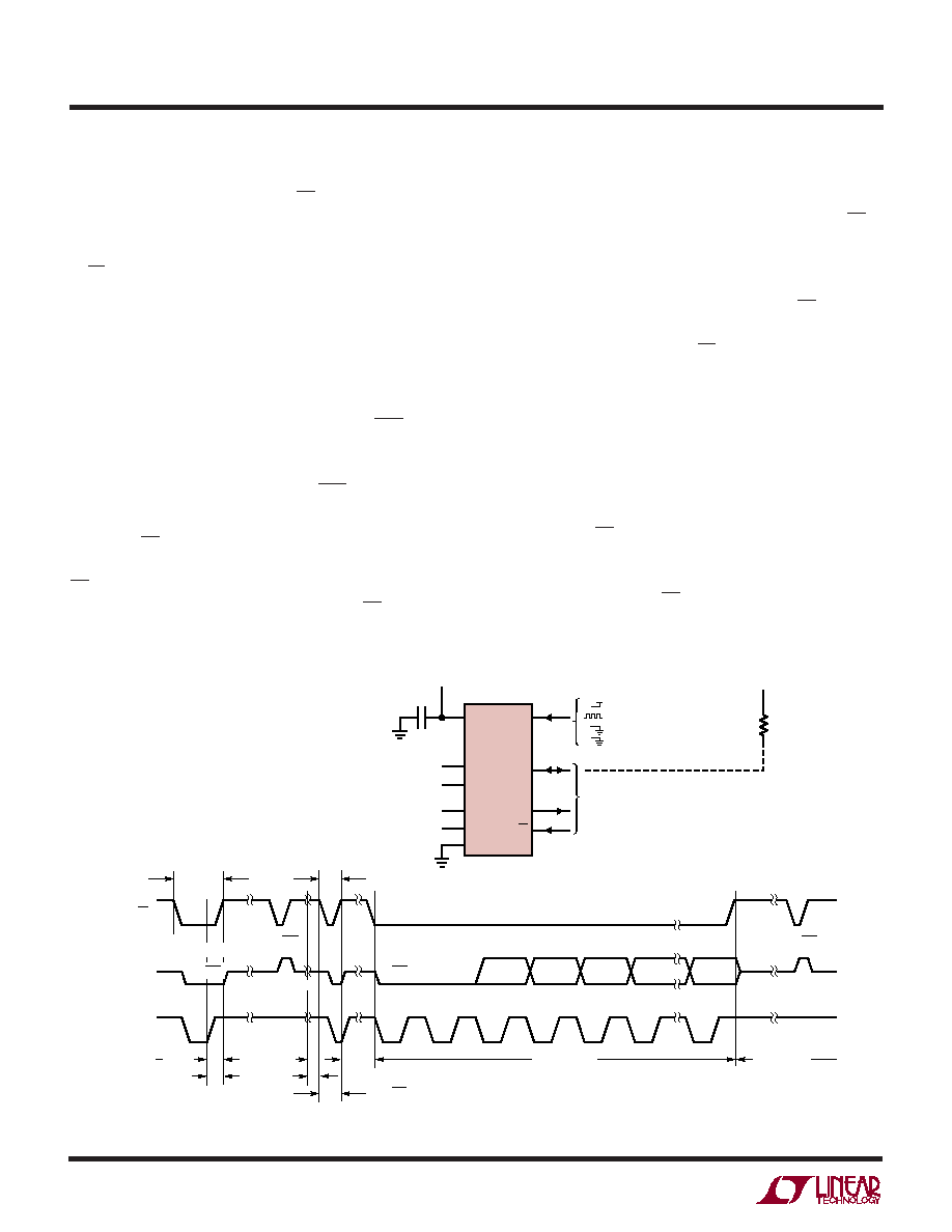
HIGH). If FO is driven by an external oscillator of frequency
fEOSC, then tEOCtest is 3.6/fEOSC. If CS is pulled HIGH before
time tEOCtest, the device returns to the sleep state. The
conversion result is held in the internal static shift register.
If CS remains LOW longer than tEOCtest, the first rising
edge of SCK will occur and the conversion result is serially
shifted out of the SDO pin. The data output cycle begins on
this first rising edge of SCK and concludes after the 24th
rising edge. Data is shifted out the SDO pin on each falling
edge of SCK. The internally generated serial clock is output
to the SCK pin. This signal may be used to shift the
conversion result into external circuitry. EOC can be
latched on the first rising edge of SCK and the last bit of the
conversion result on the 24th rising edge of SCK. After the
24th rising edge, SDO goes HIGH (EOC = 1), SCK stays
HIGH and a new conversion starts.
Typically, CS remains LOW during the data output state.
However, the data output state may be aborted by pulling
CS HIGH anytime between the first and 24th rising edge of
SCK, see Figure 12. On the rising edge of CS, the device
aborts the data output state and immediately initiates a
new conversion. This is useful for systems not requiring
all 24 bits of output data, aborting an invalid conversion
cycle, or synchronizing the start of a conversion. If CS is
pulled HIGH while the converter is driving SCK LOW, the
internal pull-up is not available to restore SCK to a logic
HIGH state. This will cause the device to exit the internal
serial clock mode on the next falling edge of CS. This can
be avoided by adding an external 10k pull-up resistor to
the SCK pin or by never pulling CS HIGH when SCK is LOW.
Whenever SCK is LOW, the LTC2435/LTC2435-1 internal
pull-up at pin SCK is disabled. Normally, SCK is not
externally driven if the device is in the internal SCK timing
mode. However, certain applications may require an exter-
nal driver on SCK. If this driver goes Hi-Z after outputting
a LOW signal, the LTC2435/LTC2435-1 internal pull-up
remains disabled. Hence, SCK remains LOW. On the next
falling edge of CS, the device is switched to the external
SCK timing mode. By adding an external 10k pull-up
resistor to SCK, this pin goes HIGH once the external driver
goes Hi-Z. On the next CS falling edge, the device will
remain in the internal SCK timing mode.
APPLICATIO S I FOR ATIO
WU
U
Figure 12. Internal Serial Clock, Reduced Data Output Length
SDO
SCK
(INTERNAL)
CS
>tEOCtest
MSB
SIG
BIT 8
TEST EOC
BIT 19
BIT 18
BIT 20
BIT 21
BIT 22
EOC
BIT 23
EOC
BIT 0
SLEEP
DATA OUTPUT
Hi-Z
DATA OUTPUT
CONVERSION
SLEEP
2435 F12
<tEOCtest
VCC
10k
TEST EOC
VCC
FO
REF+
REF–
SCK
IN+
IN–
SDO
GND
CS
214
3
4
13
5
6
12
1, 7, 8, 9, 10, 15, 16
11
REFERENCE
VOLTAGE
0.1V TO VCC
ANALOG INPUT RANGE
–0.5VREF TO 0.5VREF
3-WIRE
SPI INTERFACE
1
μF
2.7V TO 5.5V
LTC2435/
LTC2435-1
= 50Hz REJECTION (LTC2435)
= EXTERNAL OSCILLATOR
= 60Hz REJECTION (LTC2435)
= 50Hz/60Hz REJECTION (LTC2435-1)
VCC
相關(guān)PDF資料 |
PDF描述 |
|---|---|
| LT2435IGN#PBF | 1-CH 20-BIT DELTA-SIGMA ADC, SERIAL ACCESS, PDSO16 |
| LT280A | SPECIALTY ANALOG CIRCUIT, PDSO4 |
| LT3407IDD-2 | 1.6 A DUAL SWITCHING CONTROLLER, 2700 kHz SWITCHING FREQ-MAX, PDSO10 |
| LT3407IMSE-2#PBF | 1.6 A DUAL SWITCHING CONTROLLER, 2700 kHz SWITCHING FREQ-MAX, PDSO10 |
| LT3407IDD-2#TRPBF | 1.6 A DUAL SWITCHING CONTROLLER, 2700 kHz SWITCHING FREQ-MAX, PDSO10 |
相關(guān)代理商/技術(shù)參數(shù) |
參數(shù)描述 |
|---|---|
| LT24512-15E | 制造商:未知廠家 制造商全稱:未知廠家 功能描述:Analog IC |
| LT2462-SERIES | 制造商:未知廠家 制造商全稱:未知廠家 功能描述:Optoelectronic |
| LT2462XX-SERIES | 制造商:未知廠家 制造商全稱:未知廠家 功能描述:Optoelectronic |
| LT24701DBB#PBF | 制造商:IC'S/TRANSISTORS/DIO 功能描述: 制造商:IC'S/TRANSISTORS/DIODES 功能描述: |
| LT24DP | 制造商:UNBRANDED 功能描述:24MM SWIFT SPLICE LEADER TAPE (2000/BX) |
發(fā)布緊急采購,3分鐘左右您將得到回復(fù)。