- 您現(xiàn)在的位置:買賣IC網(wǎng) > PDF目錄39399 > LT2435-1CGN#PBF (LINEAR TECHNOLOGY CORP) 1-CH 20-BIT DELTA-SIGMA ADC, SERIAL ACCESS, PDSO16 PDF資料下載
參數(shù)資料
| 型號(hào): | LT2435-1CGN#PBF |
| 廠商: | LINEAR TECHNOLOGY CORP |
| 元件分類: | ADC |
| 英文描述: | 1-CH 20-BIT DELTA-SIGMA ADC, SERIAL ACCESS, PDSO16 |
| 封裝: | 0.150 INCH, LEAD FREE, PLASTIC, SSOP-16 |
| 文件頁數(shù): | 20/40頁 |
| 文件大?。?/td> | 458K |
| 代理商: | LT2435-1CGN#PBF |
第1頁第2頁第3頁第4頁第5頁第6頁第7頁第8頁第9頁第10頁第11頁第12頁第13頁第14頁第15頁第16頁第17頁第18頁第19頁當(dāng)前第20頁第21頁第22頁第23頁第24頁第25頁第26頁第27頁第28頁第29頁第30頁第31頁第32頁第33頁第34頁第35頁第36頁第37頁第38頁第39頁第40頁
LTC2435/LTC2435-1
27
24351fb
APPLICATIO S I FOR ATIO
WU
U
tance driving IN+ or IN–. When FO is driven by an external
oscillator with a frequency fEOSC (external conversion
clock operation), the typical differential input resistance is
3.3 1012/fEOSCΩ and each ohm of source resistance
driving IN+ or IN– will result in 0.15 10–6 fEOSC ppm +FS
gain error. The effect of the source resistance on the two
input pins is additive with respect to this gain error. The
typical +FS and –FS errors as a function of the sum of the
source resistance seen by IN+ and IN– for large values of
CIN are shown in Figures 18 and 19.
In addition to this gain error, an offset error term may also
appear. The offset error is proportional to the mismatch
between the source impedance driving the two input pins
IN+ and IN– and with the difference between the input and
reference common mode voltages. While the input drive
circuit nonzero source impedance combined with the
converter average input current will not degrade the INL
performance, indirect distortion may result from the modu-
lation of the offset error by the common mode component
of the input signal. Thus, when using large CIN capacitor
values, it is advisable to carefully match the source imped-
ance seen by the IN+ and IN– pins. When FO = LOW
(internal oscillator and 60Hz notch), every 1
Ω mismatch
in source impedance transforms a full-scale common
mode input signal into a differential mode input signal of
0.023ppm. When FO = HIGH (internal oscillator and 50Hz
notch), every 1
Ω mismatch in source impedance trans-
forms a full-scale common mode input signal into a
differential mode input signal of 0.02ppm. When FO is
driven by an external oscillator with a frequency fEOSC,
every 1
Ω mismatch in source impedance transforms a
full-scale common mode input signal into a differential
mode input signal of 0.15 10–6 fEOSCppm. Figure 20
shows the typical offset error due to input common mode
voltage for various values of source resistance imbalance
between the IN+ and IN– pins when large CIN values are
used.
If possible, it is desirable to operate with the input signal
common mode voltage very close to the reference signal
common mode voltage as is the case in the ratiometric
measurement of a symmetric bridge. This configuration
eliminates the offset error caused by mismatched source
impedances.
The magnitude of the dynamic input current depends upon
the size of the very stable internal sampling capacitors and
upon the accuracy of the converter sampling clock. The
accuracy of the internal clock over the entire temperature
and power supply range is typical better than 0.5%. Such
a specification can also be easily achieved by an external
clock. When relatively stable resistors (50ppm/
°C) are
used for the external source impedance seen by IN+ and
IN–, the expected drift of the dynamic current, offset and
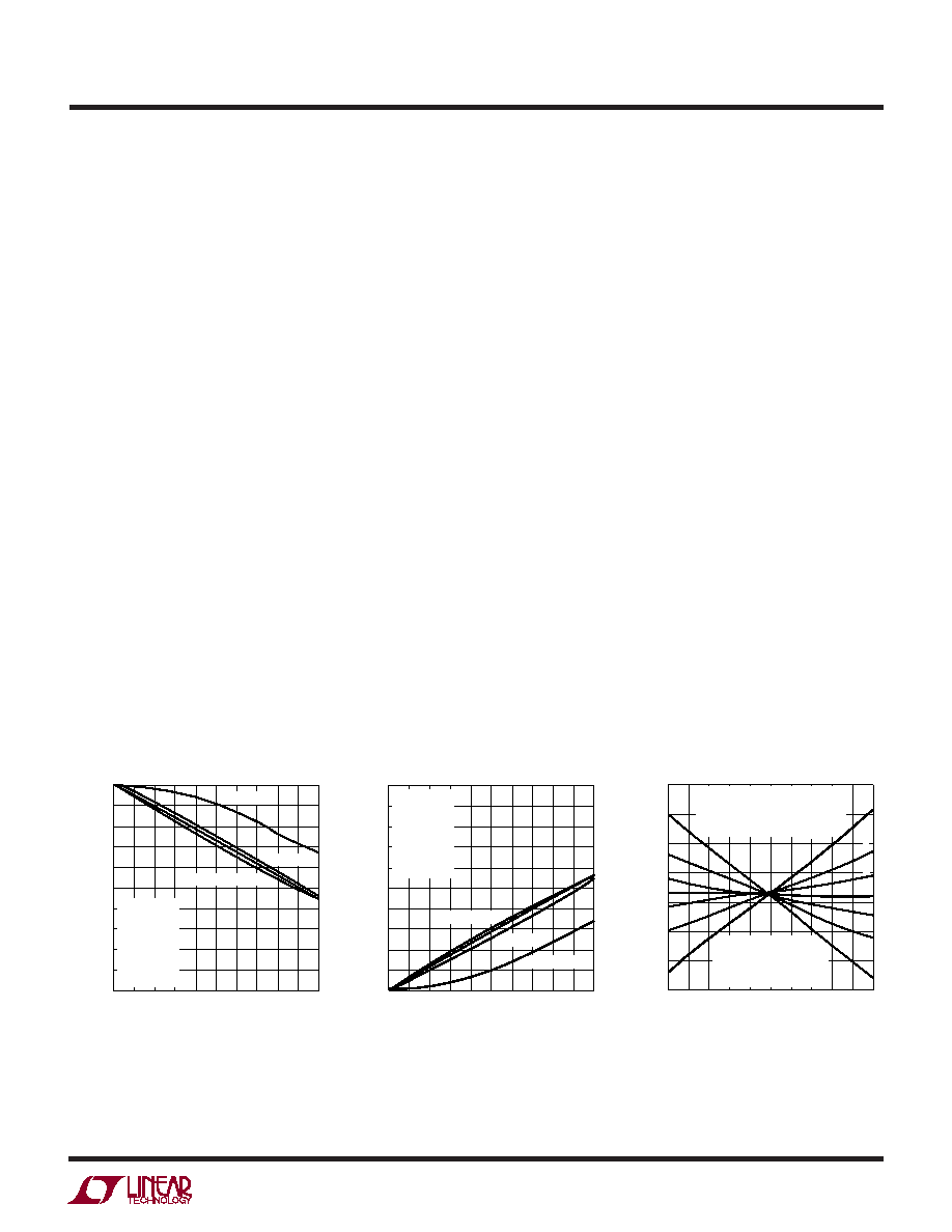
Figure 18. +FS Error vs RSOURCE
at IN+ or IN– (Large CIN)
Figure 19. –FS Error vs RSOURCE
at IN+ or IN– (Large CIN)
Figure 20. Offset Error vs Common Mode
Voltage (VINCM = VIN+ = VIN–) and Input
Source Resistance Imbalance (
ΔRIN =
RSOURCEIN+ – RSOURCEIN–) for Large CIN
Values (CIN ≥ 1μF)
RSOURCE (Ω)
0
–10
–20
–30
–40
–50
–60
–70
–80
–90
–100
+FS
ERROR
VARIATION
(ppm)
2435 F18
0
400
800
1200
1600
2000
VCC = 5V
VREF+ = 5V
VREF– = GND
VIN+ = 3.75V
VIN– = 1.25V
FO = GND
TA = 25°C
CIN = 1μF, 10μF
CIN = 0.01μF
CIN = 0.1μF
RSOURCE (Ω)
100
90
80
70
60
50
40
30
20
10
0
–
FS
ERROR
VARIATION
(ppm)
2435 F19
0
400
800
1200
1600
2000
VCC = 5V
VREF+ = 5V
VREF– = GND
VIN+ = 1.25V
VIN– = 3.75V
FO = GND
TA = 25°C
CIN = 1μF, 10μF
CIN = 0.01μF
CIN = 0.1μF
A
B
C
D
E
F
G
VINCM (V)
0
OFFSET
ERROR
(ppm)
–310
–320
–330
–340
–350
–360
–370
–380
2435 F20
2.0
5.0
1.0
3.0
4.0
0.5
2.5
1.5
3.5
4.5
VCC = 5V
VREF+ = 5V
VREF– = GND
VIN+ = VIN– = VINCM
A:
ΔRIN = 1k
B:
ΔRIN = 500Ω
C:
ΔRIN = 200Ω
D:
ΔRIN = 0Ω
E:
ΔRIN = –200Ω
F:
ΔRIN = –500Ω
G:
ΔRIN = –1k
FO = GND
TA = 25°C
CIN = 10μF
相關(guān)PDF資料 |
PDF描述 |
|---|---|
| LT2435-1IGN#PBF | 1-CH 20-BIT DELTA-SIGMA ADC, SERIAL ACCESS, PDSO16 |
| LT2435CGN#PBF | 1-CH 20-BIT DELTA-SIGMA ADC, SERIAL ACCESS, PDSO16 |
| LT2435IGN#PBF | 1-CH 20-BIT DELTA-SIGMA ADC, SERIAL ACCESS, PDSO16 |
| LT280A | SPECIALTY ANALOG CIRCUIT, PDSO4 |
| LT3407IDD-2 | 1.6 A DUAL SWITCHING CONTROLLER, 2700 kHz SWITCHING FREQ-MAX, PDSO10 |
相關(guān)代理商/技術(shù)參數(shù) |
參數(shù)描述 |
|---|---|
| LT24512-15E | 制造商:未知廠家 制造商全稱:未知廠家 功能描述:Analog IC |
| LT2462-SERIES | 制造商:未知廠家 制造商全稱:未知廠家 功能描述:Optoelectronic |
| LT2462XX-SERIES | 制造商:未知廠家 制造商全稱:未知廠家 功能描述:Optoelectronic |
| LT24701DBB#PBF | 制造商:IC'S/TRANSISTORS/DIO 功能描述: 制造商:IC'S/TRANSISTORS/DIODES 功能描述: |
| LT24DP | 制造商:UNBRANDED 功能描述:24MM SWIFT SPLICE LEADER TAPE (2000/BX) |
發(fā)布緊急采購(gòu),3分鐘左右您將得到回復(fù)。