- 您現(xiàn)在的位置:買賣IC網(wǎng) > PDF目錄39399 > LT2435-1CGN#PBF (LINEAR TECHNOLOGY CORP) 1-CH 20-BIT DELTA-SIGMA ADC, SERIAL ACCESS, PDSO16 PDF資料下載
參數(shù)資料
| 型號(hào): | LT2435-1CGN#PBF |
| 廠商: | LINEAR TECHNOLOGY CORP |
| 元件分類: | ADC |
| 英文描述: | 1-CH 20-BIT DELTA-SIGMA ADC, SERIAL ACCESS, PDSO16 |
| 封裝: | 0.150 INCH, LEAD FREE, PLASTIC, SSOP-16 |
| 文件頁數(shù): | 13/40頁 |
| 文件大小: | 458K |
| 代理商: | LT2435-1CGN#PBF |
第1頁第2頁第3頁第4頁第5頁第6頁第7頁第8頁第9頁第10頁第11頁第12頁當(dāng)前第13頁第14頁第15頁第16頁第17頁第18頁第19頁第20頁第21頁第22頁第23頁第24頁第25頁第26頁第27頁第28頁第29頁第30頁第31頁第32頁第33頁第34頁第35頁第36頁第37頁第38頁第39頁第40頁
LTC2435/LTC2435-1
20
24351fb
The external serial clock mode is selected at the end of the
power-on reset (POR) cycle. The POR cycle is concluded
approximately 1ms after VCC exceeds 2.2V. The level
applied to SCK at this time determines if SCK is internal or
external. SCK must be driven LOW prior to the end of POR
in order to enter the external serial clock timing mode.
Since CS is tied LOW, the end-of-conversion (EOC) can be
continuously monitored at the SDO pin during the convert
and sleep states. EOC may be used as an interrupt to an
external controller indicating the conversion result is
ready. EOC = 1 while the conversion is in progress and
EOC = 0 once the conversion is over. On the falling edge of
EOC, the conversion result is loaded into an internal static
shift register. Data is shifted out the SDO pin on each
falling edge of SCK enabling external circuitry to latch data
on the rising edge of SCK. EOC can be latched on the first
rising edge of SCK. On the 24th falling edge of SCK, SDO
goes HIGH (EOC = 1) indicating a new conversion has
begun.
APPLICATIO S I FOR ATIO
WU
U
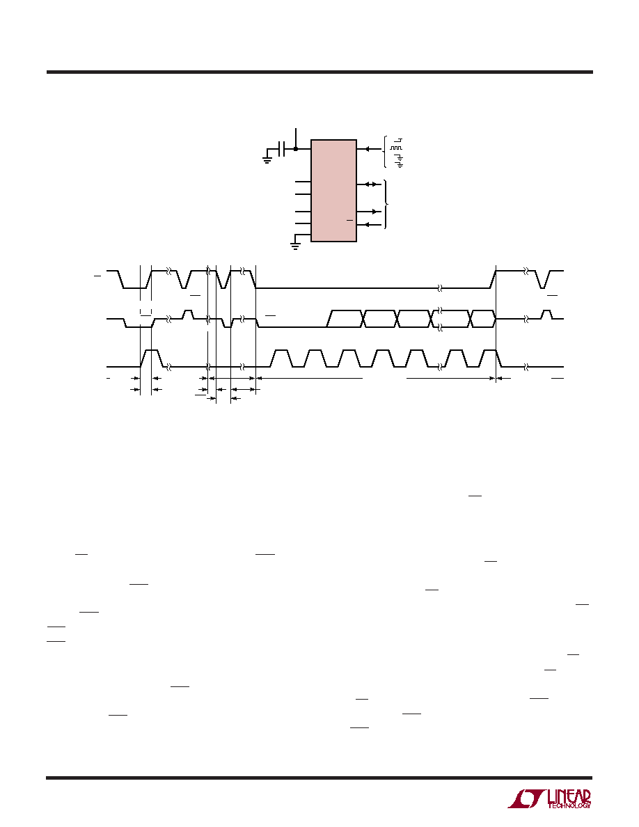
Figure 9. External Serial Clock, Reduced Data Output Length
SDO
SCK
(EXTERNAL)
CS
DATA OUTPUT
CONVERSION
SLEEP
TEST EOC
DATA OUTPUT
Hi-Z
CONVERSION
2435 F09
MSB
SIG
BIT 8
BIT 19
BIT 9
BIT 20
BIT 21
BIT 22
EOC
BIT 23
BIT 0
EOC
Hi-Z
TEST EOC
VCC
FO
REF+
REF–
SCK
IN+
IN–
SDO
GND
CS
214
3
4
13
5
6
12
1, 7, 8, 9, 10, 15, 16
11
REFERENCE
VOLTAGE
0.1V TO VCC
ANALOG INPUT RANGE
–0.5VREF TO 0.5VREF
3-WIRE
SPI INTERFACE
1
μF
2.7V TO 5.5V
LTC2435/
LTC2435-1
= 50Hz REJECTION (LTC2435)
= EXTERNAL OSCILLATOR
= 60Hz REJECTION (LTC2435)
= 50Hz/60Hz REJECTION (LTC2435-1)
VCC
Internal Serial Clock, Single Cycle Operation
This timing mode uses an internal serial clock to shift out
the conversion result and a CS signal to monitor and
control the state of the conversion cycle, see Figure 11.
In order to select the internal serial clock timing mode, the
serial clock pin (SCK) must be floating (Hi-Z) or pulled
HIGH prior to the falling edge of CS. The device will not
enter the internal serial clock mode if SCK is driven LOW
on the falling edge of CS. An internal weak pull-up resistor
is active on the SCK pin during the falling edge of CS;
therefore, the internal serial clock timing mode is auto-
matically selected if SCK is not externally driven.
The serial data output pin (SDO) is Hi-Z as long as CS is
HIGH. At any time during the conversion cycle, CS may be
pulled LOW in order to monitor the state of the converter.
Once CS is pulled LOW, SCK goes LOW and EOC is output
to the SDO pin. EOC = 1 while a conversion is in progress
and EOC = 0 if the conversion is over.
相關(guān)PDF資料 |
PDF描述 |
|---|---|
| LT2435-1IGN#PBF | 1-CH 20-BIT DELTA-SIGMA ADC, SERIAL ACCESS, PDSO16 |
| LT2435CGN#PBF | 1-CH 20-BIT DELTA-SIGMA ADC, SERIAL ACCESS, PDSO16 |
| LT2435IGN#PBF | 1-CH 20-BIT DELTA-SIGMA ADC, SERIAL ACCESS, PDSO16 |
| LT280A | SPECIALTY ANALOG CIRCUIT, PDSO4 |
| LT3407IDD-2 | 1.6 A DUAL SWITCHING CONTROLLER, 2700 kHz SWITCHING FREQ-MAX, PDSO10 |
相關(guān)代理商/技術(shù)參數(shù) |
參數(shù)描述 |
|---|---|
| LT24512-15E | 制造商:未知廠家 制造商全稱:未知廠家 功能描述:Analog IC |
| LT2462-SERIES | 制造商:未知廠家 制造商全稱:未知廠家 功能描述:Optoelectronic |
| LT2462XX-SERIES | 制造商:未知廠家 制造商全稱:未知廠家 功能描述:Optoelectronic |
| LT24701DBB#PBF | 制造商:IC'S/TRANSISTORS/DIO 功能描述: 制造商:IC'S/TRANSISTORS/DIODES 功能描述: |
| LT24DP | 制造商:UNBRANDED 功能描述:24MM SWIFT SPLICE LEADER TAPE (2000/BX) |
發(fā)布緊急采購,3分鐘左右您將得到回復(fù)。