- 您現(xiàn)在的位置:買賣IC網(wǎng) > PDF目錄377719 > LT1952IGN (LINEAR TECHNOLOGY CORP) Single Switch Synchronous Forward Controller PDF資料下載
參數(shù)資料
| 型號(hào): | LT1952IGN |
| 廠商: | LINEAR TECHNOLOGY CORP |
| 元件分類: | 穩(wěn)壓器 |
| 英文描述: | Single Switch Synchronous Forward Controller |
| 中文描述: | 1 A SWITCHING CONTROLLER, 560 kHz SWITCHING FREQ-MAX, PDSO16 |
| 封裝: | 0.150 INCH, PLASTIC, SSOP-16 |
| 文件頁數(shù): | 23/24頁 |
| 文件大小: | 252K |
| 代理商: | LT1952IGN |
LT1952
23
1952f
Information furnished by Linear Technology Corporation is believed to be accurate and reliable.
However, no responsibility is assumed for its use. Linear Technology Corporation makes no represen-
tation that the interconnection of its circuits as described herein will not infringe on existing patent rights.
APPLICATIU
Bus Converter: Optimum Output Voltage Tolerance
The Bus Converter applications shown on page 1 and in
Figure 16, provide semi-regulated isolated outputs with-
out the need for an optocoupler, optocoupler driver, refer-
ence or feedback network. The LT1952 Volt-Second clamp
adjusts switch duty cycle inversely proportional to input
voltage to provide an output voltage that is regulated against
input line variations. Some bus converters use a switch
duty cycle limit which causes output voltage variation of
typically
±
33% over a 2:1 input voltage range. The LT1952
typically provides a
±
10% output variation for the same
input variation. Typical output tolerance is further improved
for the LT1952 by inserting a resistor from the system
input voltage to the SS_MAXDC pin (Rx in Figure 19).
The LT1952 electrical specifications for the OUT Max Duty
Cycle Clamp show typical switch duty cycle to move from
72% to 33% for a 2x change of input voltage
(SS_MAXDC pin = 1.84V). Since output voltage regulation
follows V
IN
Duty Cycle, a switch duty cycle change of
72% to 36% (for a 2x input voltage change) provides
minimal output voltage variation for the LT1952 bus con-
verter. To achieve this, an SS_MAXDC pin voltage increase
of 1.09x (36/33) would be required at high input line. A
resistor Rx inserted between the SS_MAXDC pin and sys-
tem input voltage (Figure 19) increases SS_MAXDC volt-
age as input voltage increases, minimizing output voltage
variation over a 2:1 input voltage change.
The following steps determine values for Rx, R
T
and R
B
(1) Program switch duty cycle at minimum system input
voltage (V
S(MIN)
)
(a) R
T(1)
= 10k (minimum allowed to still guarantee soft-
start pull-down)
W
U
U
(b) Select switch duty cycle for the Bus Converter for a
given output voltage at V
S(MIN)
and calculate
SS_MAXDC voltage (SS1) (See Applications Informa-
tion “Programming Maximum Duty Cycle Clamp”)
(c) Calculate R
B(1)
= [SS1/(2.5 – SS1)] R
T(1)
(2) Calculate Rx
Rx = ([V
S(MAX) –
V
S(MIN)
]/[SS1 (X – 1)]) R
THEV(1)
R
THEV(1)
= R
B(1)
R
T(1)
/(R
B(1)
+ R
T(1)
), X = ideal duty
cycle (V
S(MAX)
)/actual duty cycle (V
S(MAX)
)
(3) The addition of Rx causes an increase in the original
programmed SS_MAXDC voltage SS1. A new value
for R
B(1)
should be calculated to provide a lower
SS_MAXDC voltage (SS2) to correct for this offset.
(a) SS2 = SS1 – [(V
S(MIN)
– SS1) R
THEV(1)
/Rx]
(b) R
B(2)
= [SS2/(2.5 – SS2)] R
T(1)
(4) The thevinin resistance R
THEV(1)
used to calculate Rx
should be re-established for R
T
and R
B
.
(a) R
B
(final value) = R
B(2)
(R
THEV(1)
/R
THEV(2)
)
(b) R
T
(final value) = R
T(1)
(R
THEV(1)
/R
THEV(2)
)
where R
THEV(2)
= R
B(2)
R
T(1)
/(R
B(2)
+ R
T(1)
)
Example:
For a Bus Converter running from 36V to 72V input,
V
S(MIN)
= 36V, V
S(MAX)
= 72V.
choose R
T(1)
= 10k, SS_MAXDC = SS1 = 1.84V (for 72%
duty cycle at V
S(MIN)
= 36V)
R
B(1)
= [1.84V/(2.5V – 1.84V)] 10k = 28k
R
THEV(1)
= [28k 10k/(28k + 10k)] = 7.4k
SS_MAXDC correction = 36%/33% = 1.09
Rx = [(72V – 36V)/(1.84 0.09)] 7.4k = 1.6M
SS2 = 1.84 – [(36V – 1.84) 7.4k/1.6M] = 1.682V
R
B(2)
= [1.682/(2.5 – 1.682)] 10k = 20.6k
R
THEV(2)
= [20.6k 10k/(20.6k + 10k)] = 6.7k
R
THEV(1)
/R
THEV(2)
= 7.4k/6.7k = 1.104
R
B
(final value) = 20.6k 1.104 = 22.7k (choose 22.6k)
R
T
(final value) = 10k 1.104 = 11k
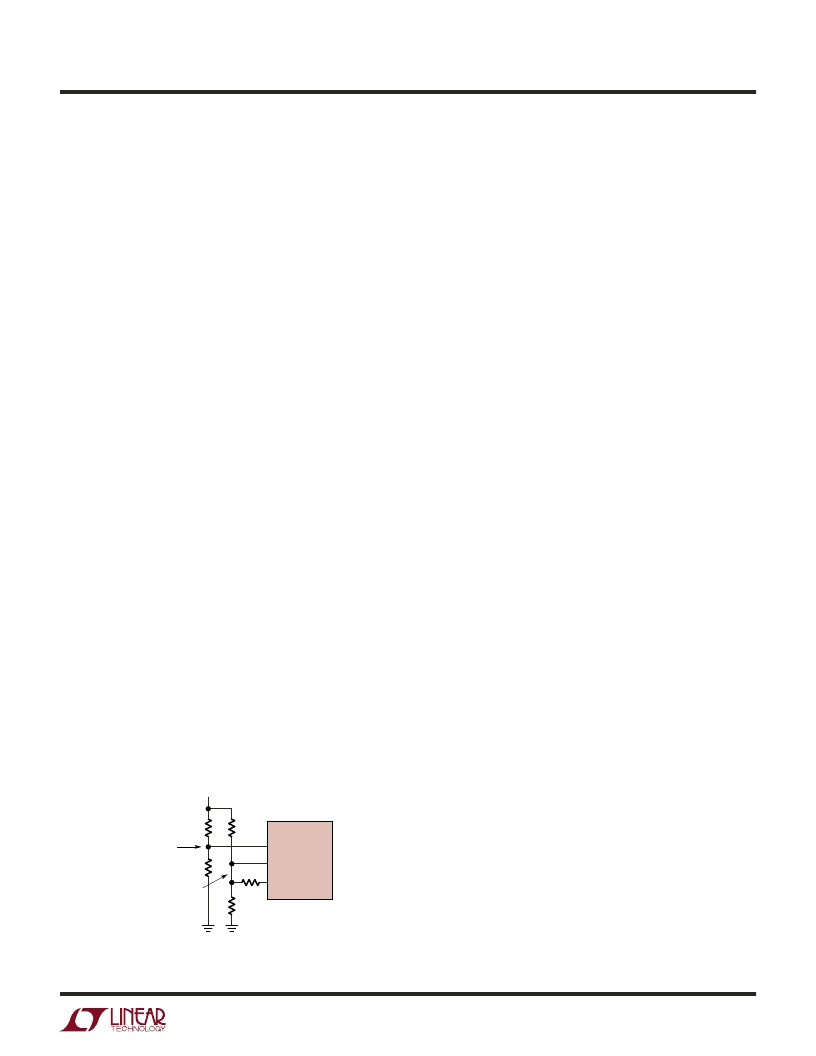
Figure 19. Optimal Programming of Maximum Duty Cycle Clamp
for Bus Converter Applications (Adding Rx)
SYSTEM
INPUT VOLTAGE
VOLT-SECOND
CLAMP INPUT
VOLT-SECOND
CLAMP ADJUST INPUT
1952 F19
SD_V
SEC
SS_MAXDC
V
REF
LT1952
R1
Rx
R2
R
B
R
T
相關(guān)PDF資料 |
PDF描述 |
|---|---|
| LT1952EGN | Single Switch Synchronous Forward Controller |
| LT1952 | Single Switch Synchronous Forward Controller |
| LT1962-1.5 | 300mA, Low Noise, Micropower LDO Regulators(1.5V輸出,300mA, 低噪聲,微功耗,低壓差輸出穩(wěn)壓器) |
| LT1962-1.8 | 300mA, Low Noise, Micropower LDO Regulators(1.8V輸出,300mA, 低噪聲,微功耗,低壓差輸出穩(wěn)壓器) |
| LT1962-2.5 | 300mA, Low Noise, Micropower LDO Regulators(2.5V輸出,300mA, 低噪聲,微功耗,低壓差輸出穩(wěn)壓器) |
相關(guān)代理商/技術(shù)參數(shù) |
參數(shù)描述 |
|---|---|
| LT1952IGN#PBF | 功能描述:IC REG CTRLR ISO PWM CM 16-SSOP RoHS:是 類別:集成電路 (IC) >> PMIC - 穩(wěn)壓器 - DC DC 切換控制器 系列:- 標(biāo)準(zhǔn)包裝:2,500 系列:- PWM 型:電流模式 輸出數(shù):1 頻率 - 最大:500kHz 占空比:96% 電源電壓:4 V ~ 36 V 降壓:無 升壓:是 回掃:無 反相:無 倍增器:無 除法器:無 Cuk:無 隔離:無 工作溫度:-40°C ~ 125°C 封裝/外殼:24-WQFN 裸露焊盤 包裝:帶卷 (TR) |
| LT1952IGN#TR | 制造商:Linear Technology 功能描述:Current Mode PWM Controller 16-Pin SSOP N T/R |
| LT1952IGN#TRPBF | 功能描述:IC REG CTRLR ISO PWM CM 16-SSOP RoHS:是 類別:集成電路 (IC) >> PMIC - 穩(wěn)壓器 - DC DC 切換控制器 系列:- 標(biāo)準(zhǔn)包裝:2,500 系列:- PWM 型:電流模式 輸出數(shù):1 頻率 - 最大:500kHz 占空比:96% 電源電壓:4 V ~ 36 V 降壓:無 升壓:是 回掃:無 反相:無 倍增器:無 除法器:無 Cuk:無 隔離:無 工作溫度:-40°C ~ 125°C 封裝/外殼:24-WQFN 裸露焊盤 包裝:帶卷 (TR) |
| LT1952IGN-1 | 制造商:Linear Technology 功能描述:Current Mode PWM Controller 16-Pin SSOP N |
| LT1952IGN-1#PBF | 功能描述:IC REG CTRLR ISO PWM CM 16-SSOP RoHS:是 類別:集成電路 (IC) >> PMIC - 穩(wěn)壓器 - DC DC 切換控制器 系列:- 特色產(chǎn)品:LM3753/54 Scalable 2-Phase Synchronous Buck Controllers 標(biāo)準(zhǔn)包裝:1 系列:PowerWise® PWM 型:電壓模式 輸出數(shù):1 頻率 - 最大:1MHz 占空比:81% 電源電壓:4.5 V ~ 18 V 降壓:是 升壓:無 回掃:無 反相:無 倍增器:無 除法器:無 Cuk:無 隔離:無 工作溫度:-5°C ~ 125°C 封裝/外殼:32-WFQFN 裸露焊盤 包裝:Digi-Reel® 產(chǎn)品目錄頁面:1303 (CN2011-ZH PDF) 其它名稱:LM3754SQDKR |
發(fā)布緊急采購,3分鐘左右您將得到回復(fù)。