- 您現(xiàn)在的位置:買賣IC網(wǎng) > PDF目錄385488 > LM6211MFX (NATIONAL SEMICONDUCTOR CORP) Low Noise, RRO Operational Amplifier with CMOS Input and 24V Operation PDF資料下載
參數(shù)資料
| 型號(hào): | LM6211MFX |
| 廠商: | NATIONAL SEMICONDUCTOR CORP |
| 元件分類: | 運(yùn)動(dòng)控制電子 |
| 英文描述: | Low Noise, RRO Operational Amplifier with CMOS Input and 24V Operation |
| 中文描述: | OP-AMP, 2800 uV OFFSET-MAX, 17 MHz BAND WIDTH, PDSO5 |
| 封裝: | SOT-23, 5 PIN |
| 文件頁數(shù): | 17/19頁 |
| 文件大小: | 1091K |
| 代理商: | LM6211MFX |
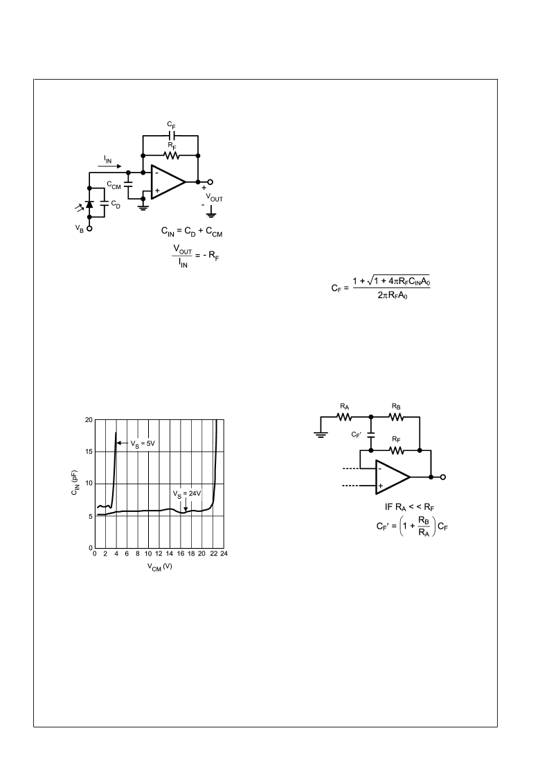
Typical Applications
(Continued)
The following parameters are used to design a transimped-
ance amplifier: the amplifier gain-bandwidth product, A
; the
amplifier input capacitance, C
; the photodiode capaci-
tance, C
D
; the transimpedance gain required, R
F
; and the
amplifier output swing. Once a feasible R
F
is selected using
the amplifier output swing, these numbers can be used to
design an amplifier with the desired transimpedance gain
and a maximally flat frequency response. The input
common-mode capacitance with respect to V
CM
for the
LM6211 is give in
Figure 14
.
An essential component for obtaining a maximally flat re-
sponse is the feedback capacitor, C
. The capacitance seen
at the input of the amplifier, C
, combined with the feedback
resistor, R
, generates a phase lag which causes gain-
peaking and can destabilize the circuit. C
is usually just the
sum of C
and C
. The feedback capacitor C
creates a
pole, f
in the noise gain of the circuit, which neutralizes the
zero in the noise gain, f
, created by the combination of R
F
and C
IN
. If properly positioned, the noise gain pole created
by C
can ensure that the slope of the gain remains at
20 dB/decade till the unity gain frequency of the amplifier is
reached, thus ensuring stability. As shown in
Figure 16
, f
is
positioned such that it coincides with the point where the
noise gain intersects the op amp’s open loop gain. In this
case, f
is also the overall 3 dB frequency of the transim-
pedance amplifier. The value of C
F
needed to make it so is
given by
Equation (2)
. A larger value of C
F
causes excessive
reduction of bandwidth, while a smaller value fails to prevent
gain peaking and maintain stability.
(2)
Calculating C
from
Equation (2)
can sometimes return un-
reasonably small values (
<
1 pF), especially for high speed
applications. In these cases, it is often more practical to use
the circuit shown in
Figure 15
in order to allow more reason-
able values. In this circuit, the capacitance C
F
’ is (1+ R
/R
)
times the effective feedback capacitance, C
F
. A larger ca-
pacitor can now be used in this circuit to obtain a smaller
effective capacitance.
For example, if a C
of 0.5 pF is needed, while only a 5 pF
capacitor is available, R
and R
can be selected such that
R
B
/R
= 9. This would convert a C
’ of 5 pF into a
C
F
of 0.5 pF. This relationship holds as long as R
A
<<
R
F
20120344
FIGURE 13. Photodiode Transimpedance Amplifier
20120354
FIGURE 14. Input Common-Mode Capacitance vs. V
CM
20120347
FIGURE 15. Modifying C
F
L
www.national.com
17
相關(guān)PDF資料 |
PDF描述 |
|---|---|
| LM62CIM3X | 2.7V, 15.6 mV/∑C SOT-23 Temperature Sensor |
| LM62BIM3 | 2.7V, 15.6 mV/∑C SOT-23 Temperature Sensor |
| LM62BIM3X | 2.7V, 15.6 mV/∑C SOT-23 Temperature Sensor |
| LM62CIM3 | 2.7V, 15.6 mV/∑C SOT-23 Temperature Sensor |
| LM6310 | High Speed Low Power Operational Amplifier with TRI-STATE Output |
相關(guān)代理商/技術(shù)參數(shù) |
參數(shù)描述 |
|---|---|
| LM6211MFX/NOPB | 功能描述:運(yùn)算放大器 - 運(yùn)放 RoHS:否 制造商:STMicroelectronics 通道數(shù)量:4 共模抑制比(最小值):63 dB 輸入補(bǔ)償電壓:1 mV 輸入偏流(最大值):10 pA 工作電源電壓:2.7 V to 5.5 V 安裝風(fēng)格:SMD/SMT 封裝 / 箱體:QFN-16 轉(zhuǎn)換速度:0.89 V/us 關(guān)閉:No 輸出電流:55 mA 最大工作溫度:+ 125 C 封裝:Reel |
| LM6218 | 制造商:未知廠家 制造商全稱:未知廠家 功能描述: |
| LM6218AH | 制造商:未知廠家 制造商全稱:未知廠家 功能描述:Voltage-Feedback Operational Amplifier |
| LM6218AJ | 制造商:未知廠家 制造商全稱:未知廠家 功能描述:Voltage-Feedback Operational Amplifier |
| LM6218AN | 制造商:NSC 制造商全稱:National Semiconductor 功能描述:Fast Settling Dual Operational Amplifiers |
發(fā)布緊急采購(gòu),3分鐘左右您將得到回復(fù)。