- 您現(xiàn)在的位置:買賣IC網(wǎng) > PDF目錄385488 > LM5104SDX (NATIONAL SEMICONDUCTOR CORP) High Voltage Half-Bridge Gate Driver with Adaptive Delay PDF資料下載
參數(shù)資料
| 型號(hào): | LM5104SDX |
| 廠商: | NATIONAL SEMICONDUCTOR CORP |
| 元件分類: | 外設(shè)及接口 |
| 英文描述: | High Voltage Half-Bridge Gate Driver with Adaptive Delay |
| 中文描述: | 1.8 A HALF BRIDGE BASED PRPHL DRVR, DSO10 |
| 封裝: | 4 X 4 MM, LLP-10 |
| 文件頁(yè)數(shù): | 9/12頁(yè) |
| 文件大小: | 375K |
| 代理商: | LM5104SDX |
Operational Description
(Continued)
The RT pin is biased at 3V and current limited to 1mA. It is
designed to accommodate a resistor between 5K and 100K,
resulting in an effective dead-time proportional to RT and
ranging from 90ns to 200ns. RT values below 5K will satu-
rate the timer and are not recommended.
Startup and UVLO
Both top and bottom drivers include under-voltage lockout
(UVLO) protection circuitry which monitors the supply volt-
age (V
) and bootstrap capacitor voltage (V
– V
)
independently. The UVLO circuit inhibits each driver until
sufficient supply voltage is available to turn-on the external
MOSFETs, and the built-in hysteresis prevents chattering
during supply voltage transitions. When the supply voltage is
applied to V
pin of LM5104, the top and bottom gates are
held low until V
exceeds UVLO threshold, typically about
6.9V. Any UVLO condition on the bootstrap capacitor will
disable only the high side output (HO).
LAYOUT CONSIDERATIONS
The optimum performance of high and low side gate drivers
cannot be achieved without taking due considerations during
circuit board layout. Following points are emphasized.
1.
A low ESR/ESL capacitor must be connected close to
the IC, and between V
DD
and V
SS
pins and between HB
and HS pins to support high peak currents being drawn
from V
DD
during turn-on of the external MOSFET.
2.
To prevent large voltage transients at the drain of the top
MOSFET, a low ESR electrolytic capacitor must be con-
nected between MOSFET drain and ground (V
SS
).
3.
In order to avoid large negative transients on the switch
node (HS) pin, the parasitic inductances in the source of
top MOSFET and in the drain of the bottom MOSFET
(synchronous rectifier) must be minimized.
4.
Grounding considerations:
a) The first priority in designing grounding connections is
to confine the high peak currents from charging and
discharging the MOSFET gate in a minimal physical
area. This will decrease the loop inductance and mini-
mize noise issues on the gate terminal of the MOSFET.
The MOSFETs should be placed as close as possible to
the gate driver.
b) The second high current path includes the bootstrap
capacitor, the bootstrap diode, the local ground refer-
enced bypass capacitor and low side MOSFET body
diode. The bootstrap capacitor is recharged on the
cycle-by-cycle basis through the bootstrap diode from
the ground referenced V
bypass capacitor. The re-
charging occurs in a short time interval and involves high
peak current. Minimizing this loop length and area on the
circuit board is important to ensure reliable operation.
5.
The resistor on the RT pin must be placed very close to
the IC and seperated from high current paths to avoid
noise coupling to the time delay generator which could
disrupt timer operation.
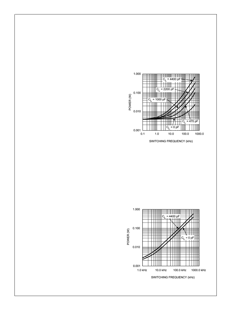
POWER DISSIPATION CONSIDERATIONS
The total IC power dissipation is the sum of the gate driver
losses and the bootstrap diode losses. The gate driver
losses are related to the switching frequency (f), output load
capacitance on LO and HO (C
), and supply voltage (V
DD
)
and can be roughly calculated as:
P
DGATES
= 2
f
C
L
V
DD2
There are some additional losses in the gate drivers due to
the internal CMOS stages used to buffer the LO and HO
outputs. The following plot shows the measured gate driver
power dissipation versus frequency and load capacitance.At
higher frequencies and load capacitance values, the power
dissipation is dominated by the power losses driving the
output loads and agrees well with the above equation. This
plot can be used to approximate the power losses due to the
gate drivers.
Gate Driver Power Dissipation (LO + HO)
V
CC
= 12V, Neglecting Diode Losses
20089006
The bootstrap diode power loss is the sum of the forward
bias power loss that occurs while charging the bootstrap
capacitor and the reverse bias power loss that occurs during
reverse recovery. Since each of these events happens once
per cycle, the diode power loss is proportional to frequency.
Larger capacitive loads require more current to recharge the
bootstrap capacitor resulting in more losses. Higher input
voltages (V
) to the half bridge result in higher reverse
recovery losses. The following plot was generated based on
calculations and lab measurements of the diode recovery
time and current under several operating conditions. This
can be useful for approximating the diode power dissipation.
Diode Power Dissipation V
IN
= 80V
20089007
L
www.national.com
9
相關(guān)PDF資料 |
PDF描述 |
|---|---|
| LM5105 | 100V Half Bridge Gate Driver with Programmable Dead-time |
| LM5105SD | 100V Half Bridge Gate Driver with Programmable Dead-time |
| LM5105SDX | 100V Half Bridge Gate Driver with Programmable Dead-time |
| LM6134AIMX | Low Power 10 MHz Rail-to-Rail I/O Operational Amplifiers |
| LM6134 | Low Power 10 MHz Rail-to-Rail I/O Operational Amplifiers |
相關(guān)代理商/技術(shù)參數(shù) |
參數(shù)描述 |
|---|---|
| LM5104SDX/NOPB | 功能描述:功率驅(qū)動(dòng)器IC RoHS:否 制造商:Micrel 產(chǎn)品:MOSFET Gate Drivers 類型:Low Cost High or Low Side MOSFET Driver 上升時(shí)間: 下降時(shí)間: 電源電壓-最大:30 V 電源電壓-最小:2.75 V 電源電流: 最大功率耗散: 最大工作溫度:+ 85 C 安裝風(fēng)格:SMD/SMT 封裝 / 箱體:SOIC-8 封裝:Tube |
| LM5105 | 制造商:NSC 制造商全稱:National Semiconductor 功能描述:100V Half Bridge Gate Driver with Programmable Dead-time |
| LM5105BSD/NOPB | 制造商:Texas Instruments 功能描述: |
| LM5105SD | 功能描述:功率驅(qū)動(dòng)器IC RoHS:否 制造商:Micrel 產(chǎn)品:MOSFET Gate Drivers 類型:Low Cost High or Low Side MOSFET Driver 上升時(shí)間: 下降時(shí)間: 電源電壓-最大:30 V 電源電壓-最小:2.75 V 電源電流: 最大功率耗散: 最大工作溫度:+ 85 C 安裝風(fēng)格:SMD/SMT 封裝 / 箱體:SOIC-8 封裝:Tube |
| LM5105SD/NOPB | 功能描述:功率驅(qū)動(dòng)器IC 100V HALF-BRIDGE DRIVER W/ DELAY RoHS:否 制造商:Micrel 產(chǎn)品:MOSFET Gate Drivers 類型:Low Cost High or Low Side MOSFET Driver 上升時(shí)間: 下降時(shí)間: 電源電壓-最大:30 V 電源電壓-最小:2.75 V 電源電流: 最大功率耗散: 最大工作溫度:+ 85 C 安裝風(fēng)格:SMD/SMT 封裝 / 箱體:SOIC-8 封裝:Tube |
發(fā)布緊急采購(gòu),3分鐘左右您將得到回復(fù)。