- 您現(xiàn)在的位置:買賣IC網(wǎng) > PDF目錄361025 > LM2744 (National Semiconductor Corporation) Low Voltage N-Channel MOSFET Synchronous Buck Regulator Controller with External Reference PDF資料下載
參數(shù)資料
| 型號: | LM2744 |
| 廠商: | National Semiconductor Corporation |
| 英文描述: | Low Voltage N-Channel MOSFET Synchronous Buck Regulator Controller with External Reference |
| 中文描述: | 低壓N溝道MOSFET同步降壓穩(wěn)壓控制器與外部參考 |
| 文件頁數(shù): | 15/22頁 |
| 文件大?。?/td> | 663K |
| 代理商: | LM2744 |
Application Information
(Continued)
down the losses in the high-side and low-side MOSFETs and
then creating spreadsheets is one way to determine relative
efficiencies between different MOSFETs. Good correlation
between the prediction and the bench is not guaranteed,
however. Single-channel buck regulators that use a control-
ler IC and discrete MOSFETs tend to be most efficient for
output currents of 2-10A.
Losses in the high-side MOSFET can be broken down into
conduction loss, gate charging loss, and switching loss.
Conduction, or I
2
R loss, is approximately:
P
C
= D (I
O2
x R
x 1.3)
(High-Side MOSFET)
P
C
= (1 - D) x (I
O2
x R
x 1.3)
(Low-Side MOSFET)
In the above equations the factor 1.3 accounts for the in-
crease in MOSFET R
due to heating. Alternatively, the
1.3 can be ignored and the R
of the MOSFET estimated
using the R
DSON
Vs. Temperature curves in the MOSFET
datasheets.
Gate charging loss results from the current driving the gate
capacitance of the power MOSFETs, and is approximated
as:
P
GC
= n x (V
DD
) x Q
G
x F
SW
where ‘n’ is the number of MOSFETs (if multiple devices
have been placed in parallel), V
DD
is the driving voltage (see
MOSFET Gate Drivers section) and Q
GS
is the gate charge
of the MOSFET. If different types of MOSFETs are used, the
‘n’ term can be ignored and their gate charges simply
summed to form a cumulative Q
G
. Gate charge loss differs
from conduction and switching losses in that the actual
dissipation occurs in the LM2744, and not in the MOSFET
itself.
Switching loss occurs during the brief transition period as the
high-side MOSFET turns on and off, during which both cur-
rent and voltage are present in the channel of the MOSFET.
It can be approximated as:
P
SW
= 0.5 x V
IN
x I
O
x (t
r
+ t
f
) x F
SW
where t
and t
are the rise and fall times of the MOSFET.
Switching loss occurs in the high-side MOSFET only.
For this example, the maximum drain-to-source voltage ap-
plied to either MOSFET is 3.6V. The maximum drive voltage
at the gate of the high-side MOSFET is 3.1V, and the maxi-
mum drive voltage for the low-side MOSFET is 3.3V. Due to
the low drive voltages in this example, a MOSFET that turns
on fully with 3.1V of gate drive is needed. For designs of 5A
and under, dual MOSFETs in SO-8 provide a good tradeoff
between size, cost, and efficiency.
Support Components
C
IN
2
- A small (0.1 to 1 μF) ceramic capacitor should be
placed as close as possible to the drain of the high-side
MOSFET and source of the low-side MOSFET (dual MOS-
FETs make this easy). This capacitor should be X5R type
dielectric or better.
R
CC
, C
CC
- These are standard filter components designed to
ensure smooth DC voltage for the chip supply. R
CC
should
be 1-10
. C
CC
should be 1 μF, X5R type or better.
C
BOOT
- Bootstrap capacitor, typically 100nF.
R
– This is a standard pull-up resistor for the open-
drain power good signal (PWGD). The recommended value
is 10 k
connected to V
. If this feature is not necessary,
the resistor can be omitted.
D
1
-Asmall Schottky diode should be used for the bootstrap.
It allows for a minimum drop for both high and low-side
drivers. The MBR0520 or BAT54 work well in most designs.
R
CS
- Resistor used to set the current limit. Since the design
calls for a peak current magnitude (I
+0.5*
I
) of 4.8A,
a safe setting would be 6A. (This is below the saturation
current of the output inductor, which is 7A.) Following the
equation from the Current Limit section, a 1.3k
resistor
should be used.
R
FADJ
- This resistor is used to set the switching frequency of
the chip. The resistor value is calculated from equation in
Normal Operation section. For 300 kHz operation, a 97.6 k
resistor should be used.
C
SS
- The soft-start capacitor depends on the user require-
ments and is calculated based on the equation given in the
section titled
START UP/SOFT-START
. Therefore, for a 7ms
delay, a 12nF capacitor is suitable.
Control Loop Compensation
The LM2744 uses voltage-mode (‘VM’) PWM control to cor-
rect changes in output voltage due to line and load tran-
sients. One of the attractive advantages of voltage mode
control is its relative immunity to noise and layout. However
VM requires careful small signal compensation of the control
loop for achieving high bandwidth and good phase margin.
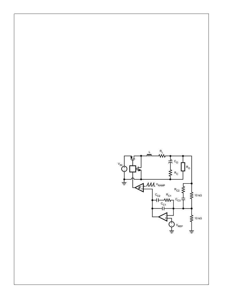
The control loop is comprised of two parts. The first is the
power stage, which consists of the duty cycle modulator,
output inductor, output capacitor, and load. The second part
is the error amplifier, which for the LM2744 is a 9MHz
op-amp used in the classic inverting configuration.
Figure 11
shows the regulator and control loop components.
One popular method for selecting the compensation compo-
nents is to create Bode plots of gain and phase for the power
stage and error amplifier. Combined, they make the overall
bandwidth and phase margin of the regulator easy to see.
Software tools such as Excel, MathCAD, and Matlab are
useful for showing how changes in compensation or the
power stage affect system gain and phase.
20106064
FIGURE 11. Power Stage and Error Amp
L
www.national.com
15
相關(guān)PDF資料 |
PDF描述 |
|---|---|
| LM2796TL | Dual-Display White LED Driver with 3/2x Switched Capacitor Boost |
| LM2796TLX | Dual-Display White LED Driver with 3/2x Switched Capacitor Boost |
| LM2796 | Dual-Display White LED Driver with 3/2x Switched Capacitor Boost |
| LM2925 | Cap-Free, NMOS, 150mA Low Dropout Regulator with Reverse Current Protection |
| LM2925T | Cap-Free, NMOS, 150mA Low Dropout Regulator with Reverse Current Protection |
相關(guān)代理商/技術(shù)參數(shù) |
參數(shù)描述 |
|---|---|
| LM2744EVAL | 功能描述:電源管理IC開發(fā)工具 EVAL BOARD RoHS:否 制造商:Maxim Integrated 產(chǎn)品:Evaluation Kits 類型:Battery Management 工具用于評估:MAX17710GB 輸入電壓: 輸出電壓:1.8 V |
| LM2744MTC | 功能描述:DC/DC 開關(guān)控制器 RoHS:否 制造商:Texas Instruments 輸入電壓:6 V to 100 V 開關(guān)頻率: 輸出電壓:1.215 V to 80 V 輸出電流:3.5 A 輸出端數(shù)量:1 最大工作溫度:+ 125 C 安裝風(fēng)格: 封裝 / 箱體:CPAK |
| LM2744MTC/NOPB | 功能描述:DC/DC 開關(guān)控制器 RoHS:否 制造商:Texas Instruments 輸入電壓:6 V to 100 V 開關(guān)頻率: 輸出電壓:1.215 V to 80 V 輸出電流:3.5 A 輸出端數(shù)量:1 最大工作溫度:+ 125 C 安裝風(fēng)格: 封裝 / 箱體:CPAK |
| LM2744MTCX | 功能描述:DC/DC 開關(guān)控制器 RoHS:否 制造商:Texas Instruments 輸入電壓:6 V to 100 V 開關(guān)頻率: 輸出電壓:1.215 V to 80 V 輸出電流:3.5 A 輸出端數(shù)量:1 最大工作溫度:+ 125 C 安裝風(fēng)格: 封裝 / 箱體:CPAK |
| LM2744MTCX/NOPB | 功能描述:DC/DC 開關(guān)控制器 RoHS:否 制造商:Texas Instruments 輸入電壓:6 V to 100 V 開關(guān)頻率: 輸出電壓:1.215 V to 80 V 輸出電流:3.5 A 輸出端數(shù)量:1 最大工作溫度:+ 125 C 安裝風(fēng)格: 封裝 / 箱體:CPAK |
發(fā)布緊急采購,3分鐘左右您將得到回復(fù)。