- 您現(xiàn)在的位置:買賣IC網(wǎng) > PDF目錄361024 > LM2599S-ADJ (NATIONAL SEMICONDUCTOR CORP) SIMPLE SWITCHER Power Converter 150 kHz 3A Step-Down Voltage Regulator, with Features PDF資料下載
參數(shù)資料
| 型號: | LM2599S-ADJ |
| 廠商: | NATIONAL SEMICONDUCTOR CORP |
| 元件分類: | 穩(wěn)壓器 |
| 英文描述: | SIMPLE SWITCHER Power Converter 150 kHz 3A Step-Down Voltage Regulator, with Features |
| 中文描述: | 7.5 A SWITCHING REGULATOR, 173 kHz SWITCHING FREQ-MAX, PSSO7 |
| 封裝: | TO-263, 7 PIN |
| 文件頁數(shù): | 23/31頁 |
| 文件大?。?/td> | 812K |
| 代理商: | LM2599S-ADJ |
第1頁第2頁第3頁第4頁第5頁第6頁第7頁第8頁第9頁第10頁第11頁第12頁第13頁第14頁第15頁第16頁第17頁第18頁第19頁第20頁第21頁第22頁當前第23頁第24頁第25頁第26頁第27頁第28頁第29頁第30頁第31頁
Application Information
(Continued)
mended (See Figure 1). The inductance required is typically
between 1 μH and 5 μH, with low DC resistance, to maintain
good load regulation.Alow ESR output filter capacitor is also
required to assure good dynamic load response and ripple
reduction. The ESR of this capacitor may be as low as de-
sired, because it is out of the regulator feedback loop. The
photo shown in Figure 19 shows a typical output ripple volt-
age, with and without a post ripple filter.
When observing output ripple with a scope, it is essential
that a short, low inductance scope probe ground connection
be used. Most scope probe manufacturers provide a special
probe terminator which is soldered onto the regulator board,
preferable at the output capacitor. This provides a very short
scope ground thus eliminating the problems associated with
the 3 inch ground lead normally provided with the probe, and
provides a much cleaner and more accurate picture of the
ripple voltage waveform.
The voltage spikes are caused by the fast switching action of
the output switch, the diode, and the parasitic inductance of
the output filter capacitor, and its associated wiring. To mini-
mize these voltage spikes, the output capacitor should be
designed for switching regulator applications, and the lead
lengths must be kept very short. Wiring inductance, stray ca-
pacitance, as well as the scope probe used to evaluate these
transients, all contribute to the amplitude of these spikes.
When a switching regulator is operating in the continuous
mode, the inductor current waveform ranges from a triangu-
lar to a sawtooth type of waveform (depending on the input
voltage). For a given input and output voltage, the
peak-to-peak amplitude of this inductor current waveform re-
mains constant. As the load current increases or decreases,
the entire sawtooth current waveform also rises and falls.
The average value (or the center) of this current waveform is
equal to the DC load current.
If the load current drops to a low enough level, the bottom of
the sawtooth current waveform will reach zero, and the
switcher will smoothly change from a continuous to a discon-
tinuous mode of operation. Most switcher designs (irregard-
less how large the inductor value is) will be forced to run dis-
continuous if the output is lightly loaded. This is a perfectly
acceptable mode of operation.
In a switching regulator design, knowing the value of the
peak-to-peak inductor ripple current (
I
) can be useful for
determining a number of other circuit parameters. Param-
eters such as, peak inductor or peak switch current, mini-
mum load current before the circuit becomes discontinuous,
output ripple voltage and output capacitor ESR can all be
calculated from the peak-to-peak
I
IND
. When the inductor
nomographs shown in Figure 4 through 7 are used to select
an inductor value, the peak-to-peak inductor ripple current
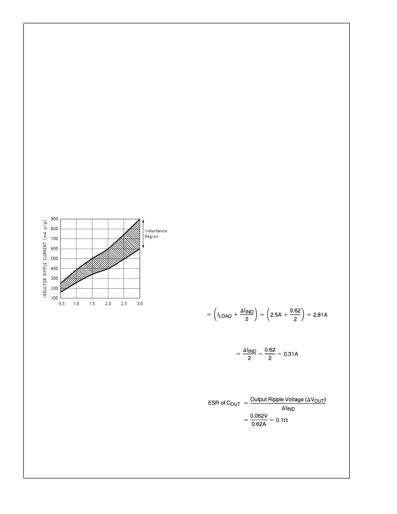
can immediately be determined. The curve shown in Figure
20shows the range of (
I
IND
) that can be expected for differ-
ent
load
currents.
The
curve
peak-to-peak inductor ripple current (
I
) changes as you
go from the lower border to the upper border (for a given load
current) within an inductance region. The upper border rep-
resents a higher input voltage, while the lower border repre-
sents a lower input voltage (see Inductor Selection Guides).
These curves are only correct for continuous mode opera-
tion, and only if the inductor selection guides are used to se-
lect the inductor value
Consider the following example:
V
OUT
= 5V, maximum load current of 2.5A
V
IN
= 12V, nominal, varying between 10V and 16V.
The selection guide in Figure 5 shows that the vertical line
for a 2.5A load current, and the horizontal line for the 12V in-
put voltage intersect approximately midway between the up-
per and lower borders of the 33 μH inductance region. A 33
μH inductor will allow a peak-to-peak inductor current (
I
)
to flow that will be a percentage of the maximum load cur-
rent. Referring to Figure 20 follow the 2.5A line approxi-
mately midway into the inductance region, and read the
peak-to-peak inductor ripple current (
I
IND
) on the left hand
axis (approximately 620 mA p-p).
As the input voltage increases to 16V, it approaches the up-
per border of the inductance region, and the inductor ripple
current increases. Referring to the curve in Figure 20 it can
be seen that for a load current of 2.5A, the peak-to-peak in-
ductor ripple current (
I
) is 620 mA with 12V in, and can
range from 740 mAat the upper border (16V in) to 500 mAat
the lower border (10V in).
Once the
I
value is known, the following formulas can be
used to calculate additional information about the switching
regulator circuit.
1.
Peak Inductor or peak switch current
also
shows
how
the
2.
Minimum load current before the circuit becomes dis-
continuous
3.
Output Ripple Voltage = (
I
IND
)x(ESR of C
OUT
)
= 0.62Ax0.1
=62 mV p-p
4.
OPEN CORE INDUCTORS
Another possible source of increased output ripple voltage or
unstable operation is from an open core inductor. Ferrite
bobbin or stick inductors have magnetic lines of flux flowing
through the air from one end of the bobbin to the other end.
DS012582-49
FIGURE 20. Peak-to-Peak Inductor
Ripple Current vs Load Current
L
www.national.com
23
相關(guān)PDF資料 |
PDF描述 |
|---|---|
| LM2599 | Octal Buffers/Drivers With 3-State Outputs 20-TSSOP -40 to 85 |
| LM2599S-5.0 | SIMPLE SWITCHER Power Converter 150 kHz 3A Step-Down Voltage Regulator, with Features |
| LM2599T-12 | SIMPLE SWITCHER Power Converter 150 kHz 3A Step-Down Voltage Regulator, with Features |
| LM2599T-3.3 | SIMPLE SWITCHER Power Converter 150 kHz 3A Step-Down Voltage Regulator, with Features |
| LM2599T-5.0 | SIMPLE SWITCHER Power Converter 150 kHz 3A Step-Down Voltage Regulator, with Features |
相關(guān)代理商/技術(shù)參數(shù) |
參數(shù)描述 |
|---|---|
| LM2599S-ADJ/NOPB | 功能描述:直流/直流開關(guān)轉(zhuǎn)換器 RoHS:否 制造商:STMicroelectronics 最大輸入電壓:4.5 V 開關(guān)頻率:1.5 MHz 輸出電壓:4.6 V 輸出電流:250 mA 輸出端數(shù)量:2 最大工作溫度:+ 85 C 安裝風格:SMD/SMT |
| LM2599SX-12 | 功能描述:直流/直流開關(guān)轉(zhuǎn)換器 RoHS:否 制造商:STMicroelectronics 最大輸入電壓:4.5 V 開關(guān)頻率:1.5 MHz 輸出電壓:4.6 V 輸出電流:250 mA 輸出端數(shù)量:2 最大工作溫度:+ 85 C 安裝風格:SMD/SMT |
| LM2599SX-12/NOPB | 功能描述:直流/直流開關(guān)轉(zhuǎn)換器 RoHS:否 制造商:STMicroelectronics 最大輸入電壓:4.5 V 開關(guān)頻率:1.5 MHz 輸出電壓:4.6 V 輸出電流:250 mA 輸出端數(shù)量:2 最大工作溫度:+ 85 C 安裝風格:SMD/SMT |
| LM2599SX-3.3 | 功能描述:直流/直流開關(guān)轉(zhuǎn)換器 RoHS:否 制造商:STMicroelectronics 最大輸入電壓:4.5 V 開關(guān)頻率:1.5 MHz 輸出電壓:4.6 V 輸出電流:250 mA 輸出端數(shù)量:2 最大工作溫度:+ 85 C 安裝風格:SMD/SMT |
| LM2599SX-3.3/NOPB | 功能描述:直流/直流開關(guān)轉(zhuǎn)換器 RoHS:否 制造商:STMicroelectronics 最大輸入電壓:4.5 V 開關(guān)頻率:1.5 MHz 輸出電壓:4.6 V 輸出電流:250 mA 輸出端數(shù)量:2 最大工作溫度:+ 85 C 安裝風格:SMD/SMT |
發(fā)布緊急采購,3分鐘左右您將得到回復。