- 您現(xiàn)在的位置:買賣IC網(wǎng) > PDF目錄39245 > LM12H458MWG-MCP (NATIONAL SEMICONDUCTOR CORP) SPECIALTY ANALOG CIRCUIT, CDFP44 PDF資料下載
參數(shù)資料
| 型號: | LM12H458MWG-MCP |
| 廠商: | NATIONAL SEMICONDUCTOR CORP |
| 元件分類: | 模擬信號調(diào)理 |
| 英文描述: | SPECIALTY ANALOG CIRCUIT, CDFP44 |
| 文件頁數(shù): | 26/43頁 |
| 文件大小: | 991K |
| 代理商: | LM12H458MWG-MCP |
第1頁第2頁第3頁第4頁第5頁第6頁第7頁第8頁第9頁第10頁第11頁第12頁第13頁第14頁第15頁第16頁第17頁第18頁第19頁第20頁第21頁第22頁第23頁第24頁第25頁當前第26頁第27頁第28頁第29頁第30頁第31頁第32頁第33頁第34頁第35頁第36頁第37頁第38頁第39頁第40頁第41頁第42頁第43頁
5.0 Analog Considerations
5.1 REFERENCE VOLTAGE
The difference in the voltages applied to the V
REF+ and
V
REF defines the analog input voltage span (the difference
between the voltages applied between two multiplexer inputs
or the voltage applied to one of the multiplexer inputs and
analog ground), over which 4095 positive and 4096 negative
codes exist. The voltage sources driving V
REF+ or VREF
must have very low output impedance and noise.
The ADC can be used in either ratiometric or absolute refer-
ence applications. In ratiometric systems, the analog input
voltage is proportional to the voltage used for the ADC’s ref-
erence voltage. When this voltage is the system power sup-
ply, the V
REF+ pin is connected to VA+ and VREF is con-
nected to GND. This technique relaxes the system reference
stability requirements because the analog input voltage and
the ADC reference voltage move together. This maintains
the same output code for given input conditions.
For absolute accuracy, where the analog input voltage varies
between very specific voltage limits, a time and temperature
stable voltage source can be connected to the reference in-
puts. Typically, the reference voltage’s magnitude will require
an initial adjustment to null reference voltage induced
full-scale errors.
When using the LM12(H)454/8’s internal 2.5V bandgap ref-
erence, a parallel combination of a 100 F capacitor and a
0.1 F capacitor connected to the V
REFOUT pin is recom-
mended for low noise operation. When left unconnected, the
reference remains stable without a bypass capacitor. How-
ever, ensure that stray capacitance at the V
REFOUT pin re-
mains below 50 pF.
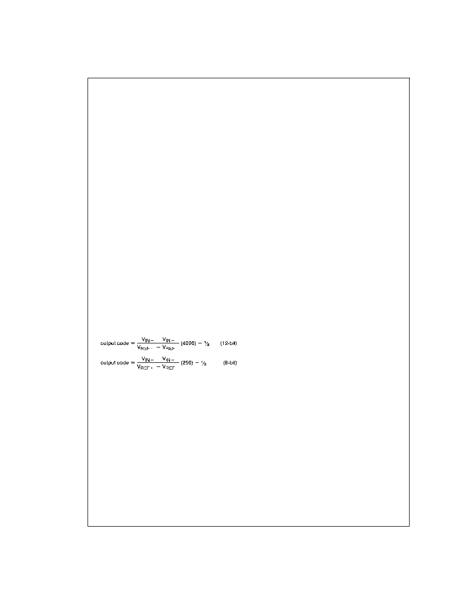
5.2 INPUT RANGE
The LM12(H)454/8’s fully differential ADC and reference
voltage inputs generate a two’s-complement output that is
found by using the equation below.
Round up to the next integer value between 4096 to 4095
for 12-bit resolution and between 256 to 255 for 8-bit reso-
lution if the result of the above equation is not a whole num-
ber. As an example, V
REF+ = 2.5V, VREF = 1V, VIN+ = 1.5V
and V
IN = GND. The 12-bit + sign output code is positive
full-scale, or 0,1111,1111,1111. If V
REF+ = 5V, VREF = 1V,
V
IN+ = 3V, and VIN = GND, the 12-bit + sign output code is
0,1100,0000,0000.
5.3 INPUT CURRENT
A charging current flows into or out of (depending on the in-
put voltage polarity) the analog input pins, IN0–IN7 at the
start of the analog input acquisition time (t
ACQ). This cur-
rent’s peak value will depend on the actual input voltage ap-
plied.
5.4 INPUT SOURCE RESISTANCE
For low impedance voltage sources (<100
for 5 MHz op-
eration and <60
for 8 MHz operation), the input charging
current will decay, before the end of the S/H’s acquisition
time, to a value that will not introduce any conversion errors.
For higher source impedances, the S/H’s acquisition time
can be increased. As an example, operating witha5MHz
clock
frequency
and
maximum
acquisition
time,
the
LM12(H)454/8’s analog inputs can handle source imped-
ance as high as 6.67 k
. When operating at 8 MHz and
maximum acquisition time, the LM12H454/8’s analog inputs
can handle source impedance as high as 4.17 k
. Refer to
Section 2.1, Instruction RAM “00”, Bits 12–15 for further in-
formation.
5.5 INPUT BYPASS CAPACITANCE
External capacitors (0.01 F–0.1 F) can be connected be-
tween the analog input pins, IN0–IN7, and analog ground to
filter any noise caused by inductive pickup associated with
long input leads. It will not degrade the conversion accuracy.
5.6 NOISE
The leads to each of the analog multiplexer input pins should
be kept as short as possible. This will minimize input noise
and clock frequency coupling that can cause conversion er-
rors. Input filtering can be used to reduce the effects of the
noise sources.
5.7 POWER SUPPLIES
Noise spikes on the V
A+ and VD+ supply lines can cause
conversion errors; the comparator will respond to the noise.
The ADC is especially sensitive to any power supply spikes
that occur during the auto-zero or linearity correction. Low in-
ductance tantalum capacitors of 10 F or greater paralleled
with 0.1 F monolithic ceramic capacitors are recommended
for supply bypassing. Separate bypass capacitors should be
used for the V
A+ and VD+ supplies and placed as close as
possible to these pins.
5.8 GROUNDING
The LM12(H)454/8’s nominal high resolution performance
can be maximized through proper grounding techniques.
These include the use of separate analog and digital ground
planes. The digital ground plane is placed under all compo-
nents that handle digital signals, while the analog ground
plane is placed under all analog signal handling circuitry. The
digital and analog ground planes are connected at only one
point, the power supply ground. This greatly reduces the oc-
currence of ground loops and noise.
It is recommended that stray capacitance between the ana-
log inputs or outputs (LM12(H)454: IN0–IN3, MUXOUT+,
MUXOUT,
S/H IN+,
S/H IN;
LM12(H)458:
IN0–IN7,
V
REF+, and VREF) be reduced by increasing the clearance
(+1/16th inch) between the analog signal and reference pins
and the ground plane.
5.9 CLOCK SIGNAL LINE ISOLATION
The LM12(H)454/8’s performance is optimized by routing the
analog input/output and reference signal conductors (pins
34–44) as far as possible from the conductor that carries the
clock signal to pin 23. Ground traces parallel to the clock sig-
nal trace can be used on printed circuit boards to reduce
clock signal interference on the analog input/output pins.
6.0 Application Circuits
PC EVALUATION/INTERFACE BOARD
Figure 16 is the schematic of an evaluation/interface board
designed to interface the LM12(H)454 or LM12(H)458 with
an XT or AT style computer. The board can be used to de-
www.national.com
32
相關(guān)PDF資料 |
PDF描述 |
|---|---|
| LM12H458MWG/883 | SPECIALTY ANALOG CIRCUIT, CDFP44 |
| LM1262NA/NOPB | 3 CHANNEL, VIDEO PREAMPLIFIER, PDIP24 |
| LM129BH/883 | 1-OUTPUT TWO TERM VOLTAGE REFERENCE, 6.9 V, MBCY2 |
| LM129BH | 1-OUTPUT TWO TERM VOLTAGE REFERENCE, 6.9 V, MBCY2 |
| LM12H454CIV | SPECIALTY ANALOG CIRCUIT, PQCC44 |
相關(guān)代理商/技術(shù)參數(shù) |
參數(shù)描述 |
|---|---|
| LM12L438CIV | 制造商:NSC 制造商全稱:National Semiconductor 功能描述:Sign Data Acquisition System with Serial I/O and Self-Calibration |
| LM12L438CIWM | 制造商:NSC 制造商全稱:National Semiconductor 功能描述:Sign Data Acquisition System with Serial I/O and Self-Calibration |
| LM12L454CIV | 制造商:Rochester Electronics LLC 功能描述:- Bulk 制造商:Texas Instruments 功能描述: |
| LM12L458 | 制造商:NSC 制造商全稱:National Semiconductor 功能描述:12-Bit + Sign Data Acquisition System with Self-Calibration |
| LM12L458_06 | 制造商:NSC 制造商全稱:National Semiconductor 功能描述:12-Bit + Sign Data Acquisition System with Self-Calibration |
發(fā)布緊急采購,3分鐘左右您將得到回復(fù)。