- 您現(xiàn)在的位置:買賣IC網(wǎng) > PDF目錄358807 > LM1202 (National Semiconductor Corporation) LM1202 230 MHz Video Amplifier System PDF資料下載
參數(shù)資料
| 型號: | LM1202 |
| 廠商: | National Semiconductor Corporation |
| 元件分類: | 視頻放大器 |
| 英文描述: | LM1202 230 MHz Video Amplifier System |
| 中文描述: | LM1202 230兆赫視頻放大器系統(tǒng) |
| 文件頁數(shù): | 7/18頁 |
| 文件大小: | 290K |
| 代理商: | LM1202 |

Circuit Description
(Continued)
VIDEO AMPLIFIER SECTION (Output Stage)
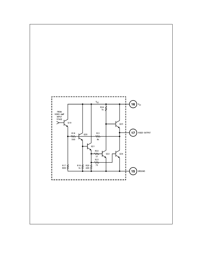
A simplified schematic of LM1202’s video amplifier output
stage is shown in Figure 4. The output stage is the second
gain stage. Ideally the gain of the second gain stage would
be A
V2
e b
R21/R18
e b
16. Because of the output
stage’s low open loop gain, the gain is approximately
A
V2
e b
10. Thus the maximum gain of the video amplifier
is A
V
e
A
V1
c
A
V2
e
20. Transistors Q23 and Q24 provide
a push-pull drive to the load. The output voltage can swing
from 0.2V to 10V.
CONTRAST CONTROL SECTION
A simplified schematic of LM1202’s contrast control section
is shown inFigure 5. A 0V to 4V DC voltage is applied at the
contrast input (pin 8). Transistors Q29, Q30 and Q34 buffer
and level shift the contrast voltage to the base of Q36. The
voltage at the emitter of Q36 equals the contrast voltage
(V
cont
) and the current through Q36’s collector is given by
I
C36
e
V
cont
/R28.
Transistor Q36’s collector current is used to unbalance the
current through the differential pair comprised of Q38
and Q40. Q40’s base is internally biased at 5.3V and made
available at pin 20. Pin 20 is externally connected to pin 1
through a 100
X
resistor (seeFigures 2 and3 ). The base of
Q38 (pin 3) is externally connected to pin 2 through a 100
X
resistor (see Figures 2 and 3 ). With V
cont
e
2V, the differ-
ential pair (Q38, Q40) is balanced and the voltage at pins 1
and 2 is 5.3V. Under this condition, Q8’s collector current is
equally split between Q9 and Q10 (see Figure 3 ) and the
amplifier’s gain is half the maximum gain. If contrast voltage
at pin 8 is greater than 2V then Q36’s collector current
increases, thus pulling Q38’s collector node lower and
consequently moving Q38’s base below 5.3V. With pin 2
at a lower voltage than pin 1, current through Q10 (see
Figure 3 ) increases and the amplifier’s gain increases. With
V
cont
e
4V, the amplifier’s gain is maximum.
If the contrast voltage at pin 8 is less than 2V then Q36’s
collector current decreases and Q38’s base is pulled above
5.3V. With pin 2 voltage greater than pin 1 voltage, less
current flows through Q10 (seeFigure 3 ), consequently the
amplifier’s gain decreases. With V
cont
e
0V, the amplifier’s
gain is minimum (i.e., maximum attenuation).
TL/H/11440–5
FIGURE 4. Simplified Schematic of LM1202 Video Amplifier Output Stage
http://www.national.com
7
相關(guān)PDF資料 |
PDF描述 |
|---|---|
| LM1202M | LM1202 230 MHz Video Amplifier System |
| LM1202N | LM1202 230 MHz Video Amplifier System |
| LM12021 | |
| LM1203C | RGB VIDEO-AMPLIFIER SYSTEM |
| LM120H-12 | Series 3-Terminal Negative Regulators |
相關(guān)代理商/技術(shù)參數(shù) |
參數(shù)描述 |
|---|---|
| LM12021 | 制造商:NSC 制造商全稱:National Semiconductor 功能描述: |
| LM1202M | 制造商:NSC 制造商全稱:National Semiconductor 功能描述:LM1202 230 MHz Video Amplifier System |
| LM1202N | 制造商:NSC 制造商全稱:National Semiconductor 功能描述:LM1202 230 MHz Video Amplifier System |
| LM1203 | 制造商:NSC 制造商全稱:National Semiconductor 功能描述:RGB Video Amplifier System |
| LM1203A | 制造商:未知廠家 制造商全稱:未知廠家 功能描述:150 MHz RGB Video Amplifier System(304.24 k) |
發(fā)布緊急采購,3分鐘左右您將得到回復。