- 您現(xiàn)在的位置:買賣IC網 > PDF目錄358807 > LM1202 (National Semiconductor Corporation) LM1202 230 MHz Video Amplifier System PDF資料下載
參數(shù)資料
| 型號: | LM1202 |
| 廠商: | National Semiconductor Corporation |
| 元件分類: | 視頻放大器 |
| 英文描述: | LM1202 230 MHz Video Amplifier System |
| 中文描述: | LM1202 230兆赫視頻放大器系統(tǒng) |
| 文件頁數(shù): | 5/18頁 |
| 文件大小: | 290K |
| 代理商: | LM1202 |

Circuit Description
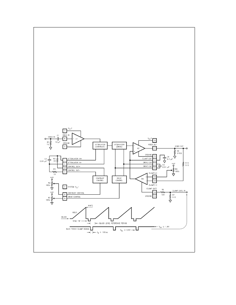
Figure 2 shows a block diagram of the LM1202 video ampli-
fier along with contrast and brightness (black level) control.
Contrast control is a DC-operated attenuator which varies
the AC gain of the amplifier. Signal attenuation (contrast) is
achieved by varying the base drive to a differential pair and
thereby unbalancing the current through the differential pair.
As shown inFigure 2, pin 20 provides a 5.3V bias voltage for
the positive input of the attenuator (pin 1). Pin 3 provides a
control voltage for the negative input (pin 2) of the attenua-
tor. The voltage at pin 3 varies as the voltage at the contrast
control input (pin 8) varies thus providing signal attenuation.
The gain is maximum (0 dB attenuation) if the voltage at pin
8 is 4V and is minimum (maximum attenuation) if the voltage
at pin 8 is 0V. The 0V to 4V DC-operated drive control at pin
9 provides a 6 dB gain adjustment range. This feature is
necessary for RGB applications where independent gain ad-
justment of each channel is required.
The brightness or black level clamping requires a ‘‘sample
and hold’’ circuit which holds the DC bias of the video ampli-
fier constant during the black level reference portion of the
video waveform. Black level clamping, often referred to as
DC restoration, is accomplished by applying a back porch
clamp signal to the clamp gate input pin (pin 14). The clamp
comparator is enabled when the clamp signal goes low dur-
ing the black level reference period (see Figure 2 ). When
the clamp comparator is enabled, the clamp capacitor con-
nected to pin 12 is either charged or discharged until the
voltage at the minus input of the comparator matches the
voltage set at the plus input of the comparator. During the
video portion of the signal, the clamp comparator is disabled
and the clamp capacitor holds the proper DC bias. In a DC
coupled cathode drive application, picture brightness func-
tion can be achieved by varying the voltage at the compara-
tor’s plus input. Note that the back porch clamp pulse width
(t
W
in Figure 2 ) must be greater than 100 ns for proper
operation.
VIDEO AMPLIFIER SECTION (Input Stage)
A simplified schematic of LM1202’s video amplifier input
stage is shown in Figure 3 . The 5.4V zener diode, Q1, Q6
and R2 bias the base of Q7 at 2.6V. The AC coupled video
signal applied to pin 6 is referenced to the 2.6V bias voltage.
Transistor Q7 buffers the video signal, V
IN
, and Q8 converts
the voltage to current. The AC collector current through Q8
is I
C8
e
V
IN
/R9. Under maximum gain condition, transistors
Q9 and Q11 are off and all of I
C8
flows through the load
resistors R10 and R11. The maximum signal gain at the
base of Q13 is, A
V1
e b
(R10
a
R11)/R9
e b
2. Signal
attenuation is achieved by varying the base drive to the dif-
ferential pairs Q9, Q10 and Q11, Q12 thereby unbalancing
the collector currents through the transistor pairs. Base of
Q10 is biased at 5.3V by externally connecting pin 1 to pin
20 through a 100
X
resistor. Pin 2 is connected to pin 3
through a 100
X
resistor. Adjusting the contrast voltage at
TL/H/11440–3
FIGURE 2. Block Diagram of the LM1202 Video Amplifier
with Contrast and Brightness (Black Level) Control
http://www.national.com
5
相關PDF資料 |
PDF描述 |
|---|---|
| LM1202M | LM1202 230 MHz Video Amplifier System |
| LM1202N | LM1202 230 MHz Video Amplifier System |
| LM12021 | |
| LM1203C | RGB VIDEO-AMPLIFIER SYSTEM |
| LM120H-12 | Series 3-Terminal Negative Regulators |
相關代理商/技術參數(shù) |
參數(shù)描述 |
|---|---|
| LM12021 | 制造商:NSC 制造商全稱:National Semiconductor 功能描述: |
| LM1202M | 制造商:NSC 制造商全稱:National Semiconductor 功能描述:LM1202 230 MHz Video Amplifier System |
| LM1202N | 制造商:NSC 制造商全稱:National Semiconductor 功能描述:LM1202 230 MHz Video Amplifier System |
| LM1203 | 制造商:NSC 制造商全稱:National Semiconductor 功能描述:RGB Video Amplifier System |
| LM1203A | 制造商:未知廠家 制造商全稱:未知廠家 功能描述:150 MHz RGB Video Amplifier System(304.24 k) |
發(fā)布緊急采購,3分鐘左右您將得到回復。