- 您現(xiàn)在的位置:買(mǎi)賣(mài)IC網(wǎng) > PDF目錄377639 > LFX200C-3F900I (Lattice Semiconductor Corporation) The ispXPGA architecture PDF資料下載
參數(shù)資料
| 型號(hào): | LFX200C-3F900I |
| 廠商: | Lattice Semiconductor Corporation |
| 英文描述: | The ispXPGA architecture |
| 中文描述: | 在ispXPGA架構(gòu) |
| 文件頁(yè)數(shù): | 32/89頁(yè) |
| 文件大小: | 941K |
| 代理商: | LFX200C-3F900I |
第1頁(yè)第2頁(yè)第3頁(yè)第4頁(yè)第5頁(yè)第6頁(yè)第7頁(yè)第8頁(yè)第9頁(yè)第10頁(yè)第11頁(yè)第12頁(yè)第13頁(yè)第14頁(yè)第15頁(yè)第16頁(yè)第17頁(yè)第18頁(yè)第19頁(yè)第20頁(yè)第21頁(yè)第22頁(yè)第23頁(yè)第24頁(yè)第25頁(yè)第26頁(yè)第27頁(yè)第28頁(yè)第29頁(yè)第30頁(yè)第31頁(yè)當(dāng)前第32頁(yè)第33頁(yè)第34頁(yè)第35頁(yè)第36頁(yè)第37頁(yè)第38頁(yè)第39頁(yè)第40頁(yè)第41頁(yè)第42頁(yè)第43頁(yè)第44頁(yè)第45頁(yè)第46頁(yè)第47頁(yè)第48頁(yè)第49頁(yè)第50頁(yè)第51頁(yè)第52頁(yè)第53頁(yè)第54頁(yè)第55頁(yè)第56頁(yè)第57頁(yè)第58頁(yè)第59頁(yè)第60頁(yè)第61頁(yè)第62頁(yè)第63頁(yè)第64頁(yè)第65頁(yè)第66頁(yè)第67頁(yè)第68頁(yè)第69頁(yè)第70頁(yè)第71頁(yè)第72頁(yè)第73頁(yè)第74頁(yè)第75頁(yè)第76頁(yè)第77頁(yè)第78頁(yè)第79頁(yè)第80頁(yè)第81頁(yè)第82頁(yè)第83頁(yè)第84頁(yè)第85頁(yè)第86頁(yè)第87頁(yè)第88頁(yè)第89頁(yè)
Lattice Semiconductor
ispXPGA Family Data Sheet
32
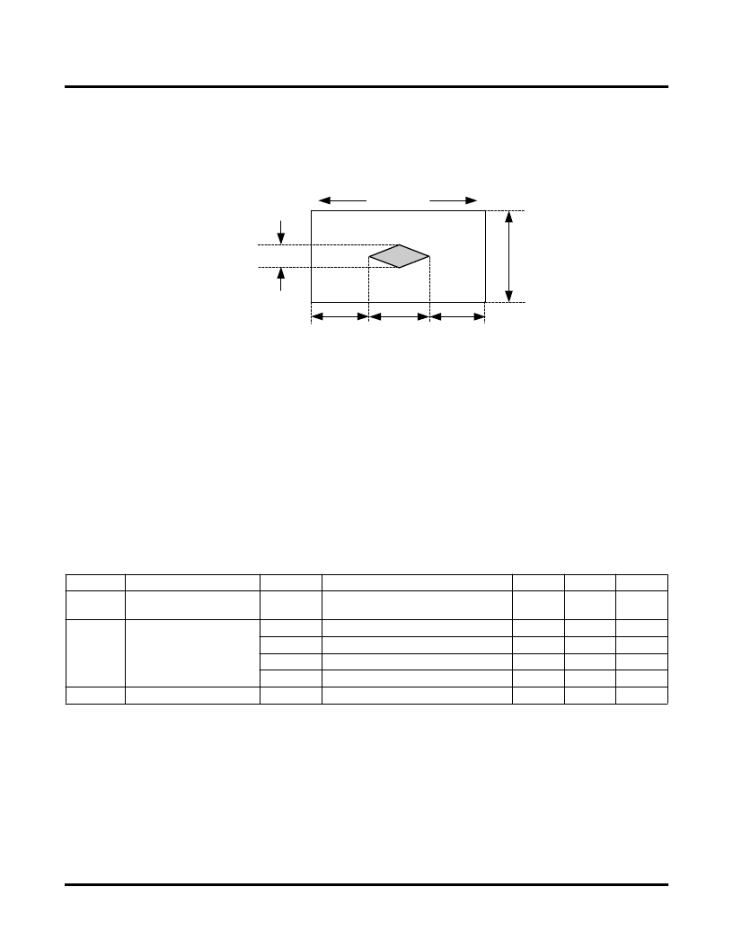
sysHSI Block Timing
Figure 23 provides a graphical representation of the SERDES receiver input requirements. It provides guidance on
a number of input parameters, including signal amplitude and rise time limits, noise and jitter limits, and P and N
input skew tolerance.
Figure 23. Receive Data Eye Diagram Template (Differential)
The data pattern eye opening at the receive end of a link is considered the ultimate measure of received signal
quality. Almost all detrimental characteristics of a transmit signal and the interconnection link design result in eye
closure. This combined with the eye-opening limitations of the line receiver can provide a good indication of a link’s
ability to transfer error-free data.
Signal jitter is of special interest to system designers. It is often the primary limiting characteristic of long digital
links and of systems with high noise level environments. An interesting characteristics of the clock and data recov-
ery (CDR) portion of the ispXPGA SERDES receiver is its ability to
fi
lter incoming signal jitter that is below the
clock recovery PLL bandwidth. For signals with high levels of low frequency jitter, the receiver can detect incoming
data error free, with eye openings signi
fi
cantly less than that shown in Figure 23.
sysHSI Block AC Speci
fi
cations
Operating Frequency Ranges
Symbol
Description
Mode
Test Condition
Min
Max
Unit
f
CLK
REFCLK, SS_CLKIN,
SS_CLKOUT
All
40
250
MHz
f
SIN
Serial Input
SS: no CAL
with eo
SIN
with eo
SIN
with eo
SIN
with eo
SIN
400
750
1
800
1
850
1
850
1
Mbps
SS: CAL
400
Mbps
10B12B
400
Mbps
8B10B
400
Mbps
f
SOUT
1. These max. numbers apply to the -4 speed grade only. For the -3 speed grade, the corresponding numbers are:
SS: no CAL 650
SS: CAL
700
10B12B
800
8B10B
800
Serial Out
LVDS
C
L
=5 pF, R
L
=100 Ohm
400
850
Mbps
EO
SIN
V
LVDT
= 200mV
JT
TH
BIT TIME
JT
TH
: Optimum Threshold Crossing Jitter
1.2 V
JT
TH
相關(guān)PDF資料 |
PDF描述 |
|---|---|
| LFX500C-4F900I | The ispXPGA architecture |
| LFX1200C-03F900C | Circular Connector; MIL SPEC:MIL-C-26482, Series I; Body Material:Aluminum Alloy; Series:MS3112; No. of Contacts:19; Connector Shell Size:14; Connecting Termination:Solder; Circular Shell Style:Box Mount Receptacle RoHS Compliant: No |
| LFX1200C-03F900I | The ispXPGA architecture |
| LFX1200C-04F900C | The ispXPGA architecture |
| LFX500C-3F900C | Circular Connector; No. of Contacts:26; Series:; Body Material:Aluminum; Connecting Termination:Solder; Connector Shell Size:16; Circular Contact Gender:Socket; Circular Shell Style:Box Mount Receptacle; Insert Arrangement:16-26 RoHS Compliant: No |
相關(guān)代理商/技術(shù)參數(shù) |
參數(shù)描述 |
|---|---|
| LFX200C-3FE680C | 制造商:LATTICE 制造商全稱(chēng):Lattice Semiconductor 功能描述:ispXPGA Family |
| LFX200C-3FE680I | 制造商:LATTICE 制造商全稱(chēng):Lattice Semiconductor 功能描述:ispXPGA Family |
| LFX200C-3FH516C | 制造商:LATTICE 制造商全稱(chēng):Lattice Semiconductor 功能描述:ispXPGA Family |
| LFX200C-3FH516I | 制造商:LATTICE 制造商全稱(chēng):Lattice Semiconductor 功能描述:ispXPGA Family |
| LFX200C-3FN256C | 制造商:LATTICE 制造商全稱(chēng):Lattice Semiconductor 功能描述:ispXPGA Family |
發(fā)布緊急采購(gòu),3分鐘左右您將得到回復(fù)。