- 您現(xiàn)在的位置:買賣IC網(wǎng) > PDF目錄377640 > LFX125C-3F900C (Lattice Semiconductor Corporation) The ispXPGA architecture PDF資料下載
參數(shù)資料
| 型號: | LFX125C-3F900C |
| 廠商: | Lattice Semiconductor Corporation |
| 英文描述: | The ispXPGA architecture |
| 中文描述: | 在ispXPGA架構(gòu) |
| 文件頁數(shù): | 14/89頁 |
| 文件大小: | 941K |
| 代理商: | LFX125C-3F900C |
第1頁第2頁第3頁第4頁第5頁第6頁第7頁第8頁第9頁第10頁第11頁第12頁第13頁當前第14頁第15頁第16頁第17頁第18頁第19頁第20頁第21頁第22頁第23頁第24頁第25頁第26頁第27頁第28頁第29頁第30頁第31頁第32頁第33頁第34頁第35頁第36頁第37頁第38頁第39頁第40頁第41頁第42頁第43頁第44頁第45頁第46頁第47頁第48頁第49頁第50頁第51頁第52頁第53頁第54頁第55頁第56頁第57頁第58頁第59頁第60頁第61頁第62頁第63頁第64頁第65頁第66頁第67頁第68頁第69頁第70頁第71頁第72頁第73頁第74頁第75頁第76頁第77頁第78頁第79頁第80頁第81頁第82頁第83頁第84頁第85頁第86頁第87頁第88頁第89頁
Lattice Semiconductor
ispXPGA Family Data Sheet
14
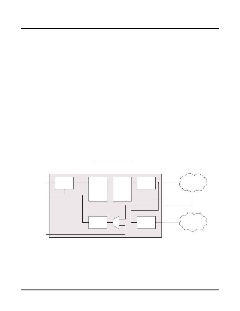
sysCLOCK PLL Description
The sysCLOCK PLL circuitry consists of Phase-Lock Loops (PLLs) and the various dividers, reset, and feedback
signals associated with the PLLs. This feature gives the user the ability to synthesize clock frequencies and gener-
ate multiple clock signals for routing within the device. Furthermore, it can generate clock signals that are aligned
either at the board level or the device level.
The ispXPGA devices provide up to eight PLLs. Each PLL receives its input clock from its associated global clock
pin, and its output is routed to the associated global clock net. For example, PLL0 receives its clock input from the
GCLK0 global clock pin and provides output to the CLK0 global clock net. The PLL also has the ability to output a
secondary clock that is a division of the primary clock output. When using the secondary clock, the secondary
clock will be routed to the neighboring global clock net. For example, PLL0 will drive its primary clock output on the
CLK0 global clock net and its secondary clock output will drive the CLK1 global clock net. Additionally, each PLL
has a set of PLL_RST, PLL_FBK, and PLL_LOCK signals. The PLL_RST signal can be generated through routing
or a dedicated dual-function I/O pin. The PLL_FBK signal can be generated through a dedicated dual-function I/O
pin or internally from the Global Clock net associated with the PLL. The PLL_LOCK signal feeds routing directly
from the sysCLOCK PLL circuit. Figure 17 illustrates how the PLL_RST and PLL_FBK signals are generated.
Each PLL has four dividers associated with it, M, N, V, and K. The M divider is used to divide the clock signal, while
the N divider is used to multiply the clock signal. The V divider allows the VCO frequency to operate at higher fre-
quencies than the clock output, thereby increasing the frequency range. The K divider is only used when a sec-
ondary clock output is needed. This divider divides the primary clock output and feeds to the adjacent global clock
net. Different combinations of these dividers allow the user to synthesize clock frequencies. Figure 16 shows the
ispXPGA PLL block diagram.
The PLL also has a delay feature that allows the output clock to be advanced or delayed to improve set-up and
clock-to-out times for better performance. This operates by inserting delay on the input or feedback lines of the
PLL. For more information on the PLL, please refer to Lattice technical note number TN1003,
Usage and Design Guidelines,
available at www.latticesemi.com.
sysCLOCK PLL
Figure 16. ispXPGA PLL Block Diagram
SEC_OUT
CLK_OUT
PLL_LOCK
GCLK_IN
PLL_RST
PLL_FBK
Input Clock
(M) Divider
Post-scalar
(V) Divider
PLL
Programable
Delay
Secondary
Clock
(K) Divider
Feedback
Loop
(N) Divider
Clock Net
Clock Net
相關(guān)PDF資料 |
PDF描述 |
|---|---|
| LFX125B-3F900I | The ispXPGA architecture |
| LFX125B-4F900I | The ispXPGA architecture |
| LFX200B-4F900I | The ispXPGA architecture |
| LFX500B-4F900I | The ispXPGA architecture |
| LG-205 | Photointerrupters(Transmissive) |
相關(guān)代理商/技術(shù)參數(shù) |
參數(shù)描述 |
|---|---|
| LFX125C-3F900I | 制造商:LATTICE 制造商全稱:Lattice Semiconductor 功能描述:The ispXPGA architecture |
| LFX125C-3FE680C | 制造商:LATTICE 制造商全稱:Lattice Semiconductor 功能描述:ispXPGA Family |
| LFX125C-3FE680I | 制造商:LATTICE 制造商全稱:Lattice Semiconductor 功能描述:ispXPGA Family |
| LFX125C-3FH516C | 制造商:LATTICE 制造商全稱:Lattice Semiconductor 功能描述:ispXPGA Family |
| LFX125C-3FH516I | 制造商:LATTICE 制造商全稱:Lattice Semiconductor 功能描述:ispXPGA Family |
發(fā)布緊急采購,3分鐘左右您將得到回復。