- 您現(xiàn)在的位置:買賣IC網(wǎng) > PDF目錄377639 > LFX1200C-04F900C (LATTICE SEMICONDUCTOR CORP) The ispXPGA architecture PDF資料下載
參數(shù)資料
| 型號: | LFX1200C-04F900C |
| 廠商: | LATTICE SEMICONDUCTOR CORP |
| 元件分類: | FPGA |
| 英文描述: | The ispXPGA architecture |
| 中文描述: | FPGA, 3844 CLBS, 1250000 GATES, PBGA900 |
| 封裝: | FPBGA-900 |
| 文件頁數(shù): | 10/89頁 |
| 文件大?。?/td> | 941K |
| 代理商: | LFX1200C-04F900C |
第1頁第2頁第3頁第4頁第5頁第6頁第7頁第8頁第9頁當(dāng)前第10頁第11頁第12頁第13頁第14頁第15頁第16頁第17頁第18頁第19頁第20頁第21頁第22頁第23頁第24頁第25頁第26頁第27頁第28頁第29頁第30頁第31頁第32頁第33頁第34頁第35頁第36頁第37頁第38頁第39頁第40頁第41頁第42頁第43頁第44頁第45頁第46頁第47頁第48頁第49頁第50頁第51頁第52頁第53頁第54頁第55頁第56頁第57頁第58頁第59頁第60頁第61頁第62頁第63頁第64頁第65頁第66頁第67頁第68頁第69頁第70頁第71頁第72頁第73頁第74頁第75頁第76頁第77頁第78頁第79頁第80頁第81頁第82頁第83頁第84頁第85頁第86頁第87頁第88頁第89頁
Lattice Semiconductor
ispXPGA Family Data Sheet
10
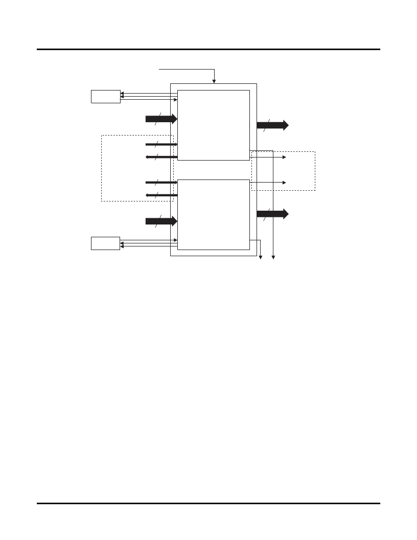
Figure 10. ispXPGA PIC
Programmable Input/Output
The PIO is the building block of a PIC. The PIO has a total of 11 inputs and
fi
ve outputs. Nine of the 11 inputs are
generated from routing. The inputs from routing are the PIO Input (IN), Feed-Thru (FT), Clock (CLK), Input Clock
Enable (ICE), Input Set/Reset (ISR), Output Clock Enable (OCEN), Output Set/Reset (OSR), PIO Output Enable
(OEN), and PIO Input Enable (IEN). The remaining inputs are the sysIO input buffer signal and the Global Set/
Reset signal. Three of the
fi
ve outputs (OUT0, OUT1, and OE) feed routing. The last two outputs feed the sysIO
buffer directly as the output and output enable of the sysIO output buffer.
PIOs associated with sysHSI blocks contain two additional inputs and outputs to support the sysHSI block. The two
inputs come from the sysHSI block associated with the PIO, and the two outputs feed the sysHSI block. One of the
inputs routes directly through the PIO to routing, while the other is multiplexed with the Feed-Thru, register bypass,
and Q output of the register to form the OUT1 output of the PIO. The outputs to the sysHSI block are the same sig-
nals as the outputs which feed the sysIO buffers (sysIO Output and sysIO Output Enable).
Each PIO has an input register, an output register, and an output enable register as shown in Figure 11. The input
register path of the PIO has a ‘delay’ option, which slows the data-
fl
ow. A two-input OR function of the Global Set/
Reset (GSR) and Set/Reset (ISR or OSR) signals creates the set/reset term for the respective registers. Each PIO
has two pairs of set/reset and clock enable signals. One is exclusive to the input register, whereas the other is com-
mon for both the output and output enable registers. The clock (CLK) is common to all registers in a PIO, and the
polarity of the clock is controllable. The input, output, and the output enable registers can be con
fi
gured as a latch
or D-type
fl
ip-
fl
op. Each PIO is capable of generating an output enable signal, which in turn becomes a PIC output.
PIC
PIO0
PIO1
OE1 OE0
sysIO
9
2
2
To routing
Only for PICs
associated with
sysHSI blocks
Only for PICs
associated with
sysHSI blocks
To routing
To routing
To routing
From routing
From routing
GSR
sysIO
From sysHSI block
To sysHSI block
2
2
9
From sysHSI block
To sysHSI block
2
2
相關(guān)PDF資料 |
PDF描述 |
|---|---|
| LFX500C-3F900C | Circular Connector; No. of Contacts:26; Series:; Body Material:Aluminum; Connecting Termination:Solder; Connector Shell Size:16; Circular Contact Gender:Socket; Circular Shell Style:Box Mount Receptacle; Insert Arrangement:16-26 RoHS Compliant: No |
| LFX1200C-3F900C | Circular Connector; No. of Contacts:26; Series:; Body Material:Aluminum; Connecting Termination:Solder; Connector Shell Size:16; Circular Contact Gender:Socket; Circular Shell Style:Box Mount Receptacle; Insert Arrangement:16-26 RoHS Compliant: No |
| LFX500C-3F900I | Circular Connector; No. of Contacts:26; Series:; Body Material:Aluminum; Connecting Termination:Solder; Connector Shell Size:16; Circular Contact Gender:Socket; Circular Shell Style:Box Mount Receptacle; Insert Arrangement:16-26 RoHS Compliant: No |
| LFX1200C-3F900I | The ispXPGA architecture |
| LFX200C-4F900C | Circular Connector; Body Material:Aluminum Alloy; Series:MS3112; No. of Contacts:8; Connector Shell Size:16; Connecting Termination:Solder; Circular Shell Style:Box Mount Receptacle; Circular Contact Gender:Pin RoHS Compliant: No |
相關(guān)代理商/技術(shù)參數(shù) |
參數(shù)描述 |
|---|---|
| LFX1200C-04FE680C | 功能描述:FPGA - 現(xiàn)場可編程門陣列 15376 LUT-4 496 I/O RoHS:否 制造商:Altera Corporation 系列:Cyclone V E 柵極數(shù)量: 邏輯塊數(shù)量:943 內(nèi)嵌式塊RAM - EBR:1956 kbit 輸入/輸出端數(shù)量:128 最大工作頻率:800 MHz 工作電源電壓:1.1 V 最大工作溫度:+ 70 C 安裝風(fēng)格:SMD/SMT 封裝 / 箱體:FBGA-256 |
| LFX1200C-04FEN680C | 功能描述:FPGA - 現(xiàn)場可編程門陣列 1.25M Gt ispJTAG 1. 8V -4 Spd RoHS:否 制造商:Altera Corporation 系列:Cyclone V E 柵極數(shù)量: 邏輯塊數(shù)量:943 內(nèi)嵌式塊RAM - EBR:1956 kbit 輸入/輸出端數(shù)量:128 最大工作頻率:800 MHz 工作電源電壓:1.1 V 最大工作溫度:+ 70 C 安裝風(fēng)格:SMD/SMT 封裝 / 箱體:FBGA-256 |
| LFX1200C-04FEN680C2 | 功能描述:FPGA - 現(xiàn)場可編程門陣列 15376 LUT-4 496 I/O RoHS:否 制造商:Altera Corporation 系列:Cyclone V E 柵極數(shù)量: 邏輯塊數(shù)量:943 內(nèi)嵌式塊RAM - EBR:1956 kbit 輸入/輸出端數(shù)量:128 最大工作頻率:800 MHz 工作電源電壓:1.1 V 最大工作溫度:+ 70 C 安裝風(fēng)格:SMD/SMT 封裝 / 箱體:FBGA-256 |
| LFX1200C-3F256C | 制造商:LATTICE 制造商全稱:Lattice Semiconductor 功能描述:ispXPGA Family |
| LFX1200C-3F256I | 制造商:LATTICE 制造商全稱:Lattice Semiconductor 功能描述:ispXPGA Family |
發(fā)布緊急采購,3分鐘左右您將得到回復(fù)。