- 您現(xiàn)在的位置:買賣IC網(wǎng) > PDF目錄377634 > LFECP6E-3T100I (Lattice Semiconductor Corporation) LatticeECP/EC Family Data Sheet PDF資料下載
參數(shù)資料
| 型號(hào): | LFECP6E-3T100I |
| 廠商: | Lattice Semiconductor Corporation |
| 英文描述: | LatticeECP/EC Family Data Sheet |
| 中文描述: | LatticeECP / EC的系列數(shù)據(jù)手冊 |
| 文件頁數(shù): | 21/117頁 |
| 文件大?。?/td> | 557K |
| 代理商: | LFECP6E-3T100I |
第1頁第2頁第3頁第4頁第5頁第6頁第7頁第8頁第9頁第10頁第11頁第12頁第13頁第14頁第15頁第16頁第17頁第18頁第19頁第20頁當(dāng)前第21頁第22頁第23頁第24頁第25頁第26頁第27頁第28頁第29頁第30頁第31頁第32頁第33頁第34頁第35頁第36頁第37頁第38頁第39頁第40頁第41頁第42頁第43頁第44頁第45頁第46頁第47頁第48頁第49頁第50頁第51頁第52頁第53頁第54頁第55頁第56頁第57頁第58頁第59頁第60頁第61頁第62頁第63頁第64頁第65頁第66頁第67頁第68頁第69頁第70頁第71頁第72頁第73頁第74頁第75頁第76頁第77頁第78頁第79頁第80頁第81頁第82頁第83頁第84頁第85頁第86頁第87頁第88頁第89頁第90頁第91頁第92頁第93頁第94頁第95頁第96頁第97頁第98頁第99頁第100頁第101頁第102頁第103頁第104頁第105頁第106頁第107頁第108頁第109頁第110頁第111頁第112頁第113頁第114頁第115頁第116頁第117頁
2-18
Architecture
Lattice Semiconductor
LatticeECP/EC Family Data Sheet
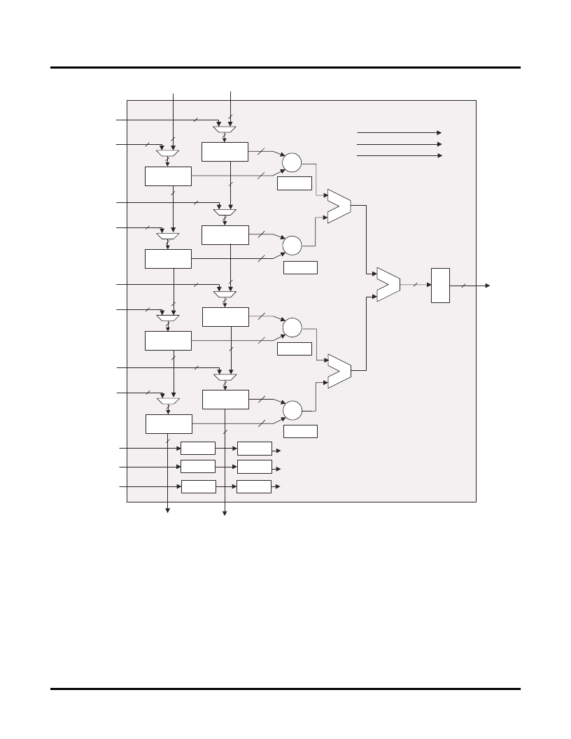
Figure 2-21. MULTADDSUM
Clock, Clock Enable and Reset Resources
Global Clock, Clock Enable and Reset signals from routing are available to every DSP block. Four Clock, Reset
and Clock Enable signals are selected for the sysDSP block. From four clock sources (CLK0, CLK1, CLK2, CLK3)
one clock is selected for each input register, pipeline register and output register. Similarly Clock enable (CE) and
Reset (RST) are selected from their four respective sources (CE0, CE1, CE2, CE3 and RST0, RST1, RST2, RST3)
at each input register, pipeline register and output register.
Signed and Unsigned with Different Widths
The DSP block supports different widths of signed and unsigned multipliers besides x9, x18 and x36 widths. For
unsigned operands, unused upper data bits should be
fi
lled to create a valid x9, x18 or x36 operand. For signed
two’s complement operands, sign extension of the most signi
fi
cant bit should be performed until x9, x18 or x36
width is reached. Table 2-8 provides an example of this.
Multiplier
x
Add/Sub0
n
m
m+n
(default)
m+n
(default)
m+n+1
m+n+2
m+n+2
m+n+1
m+n
(default)
m+n
(default)
m
n
m
n
m
n
n
m
x
n
n
m
n
n
m
Multiplier
x
Multiplier
Multiplier
x
Add/Sub1
n
m
m
n
m
n
m
n
n
m
n
m
m
n
m
n
n
m
SUM
Multiplier B0
Multiplicand A0
Multiplier B1
Multiplicand A1
Multiplier B2
Multiplicand A2
Multiplier B3
Multiplicand A3
Signed
Shift Register B In
Output
Addn0
Pipeline
Register
CLK (CLK0,CLK1,CLK2,CLK3)
CE (CE0,CE1,CE2,CE3)
RST(RST0,RST1,RST2,RST3)
Input
Register
Pipeline
Register
Input
Register
To Add/Sub0
To Add/Sub0, Add/Sub1
Pipeline
Register
Pipeline
Register
Input
Register
To Add/Sub1
Addn1
Pipeline
Register
Pipeline
Register
Pipeline
Register
Shift Register A In
Shift Register B Out
Shift Register A Out
Input Data
Register A
Input Data
Register A
Input Data
Register A
Input Data
Register A
Input Data
Register B
Input Data
Register B
Input Data
Register B
Input Data
Register B
O
R
相關(guān)PDF資料 |
PDF描述 |
|---|---|
| LFECP6E-3T144C | LatticeECP/EC Family Data Sheet |
| LFECP6E-3T144I | LatticeECP/EC Family Data Sheet |
| LFECP6E-4F256C | Quad Low-Power Low-Voltage Operational Amplifier 14-SOIC |
| LFECP6E-4F256I | LatticeECP/EC Family Data Sheet |
| LFECP6E-4F484C | LatticeECP/EC Family Data Sheet |
相關(guān)代理商/技術(shù)參數(shù) |
參數(shù)描述 |
|---|---|
| LFECP6E-3T144C | 功能描述:FPGA - 現(xiàn)場可編程門陣列 6.1 LUT 97 I/O RoHS:否 制造商:Altera Corporation 系列:Cyclone V E 柵極數(shù)量: 邏輯塊數(shù)量:943 內(nèi)嵌式塊RAM - EBR:1956 kbit 輸入/輸出端數(shù)量:128 最大工作頻率:800 MHz 工作電源電壓:1.1 V 最大工作溫度:+ 70 C 安裝風(fēng)格:SMD/SMT 封裝 / 箱體:FBGA-256 |
| LFECP6E-3T144I | 功能描述:FPGA - 現(xiàn)場可編程門陣列 6.1 LUT 97 I/O RoHS:否 制造商:Altera Corporation 系列:Cyclone V E 柵極數(shù)量: 邏輯塊數(shù)量:943 內(nèi)嵌式塊RAM - EBR:1956 kbit 輸入/輸出端數(shù)量:128 最大工作頻率:800 MHz 工作電源電壓:1.1 V 最大工作溫度:+ 70 C 安裝風(fēng)格:SMD/SMT 封裝 / 箱體:FBGA-256 |
| LFECP6E-3TN100C | 制造商:LATTICE 制造商全稱:Lattice Semiconductor 功能描述:LatticeECP/EC Family Data Sheet |
| LFECP6E-3TN100I | 制造商:LATTICE 制造商全稱:Lattice Semiconductor 功能描述:LatticeECP/EC Family Data Sheet |
| LFECP6E-3TN144C | 功能描述:FPGA - 現(xiàn)場可編程門陣列 6.1 LUT 97 I/O RoHS:否 制造商:Altera Corporation 系列:Cyclone V E 柵極數(shù)量: 邏輯塊數(shù)量:943 內(nèi)嵌式塊RAM - EBR:1956 kbit 輸入/輸出端數(shù)量:128 最大工作頻率:800 MHz 工作電源電壓:1.1 V 最大工作溫度:+ 70 C 安裝風(fēng)格:SMD/SMT 封裝 / 箱體:FBGA-256 |
發(fā)布緊急采購,3分鐘左右您將得到回復(fù)。