- 您現(xiàn)在的位置:買賣IC網(wǎng) > PDF目錄377635 > LFECP33E-3F672C (LATTICE SEMICONDUCTOR CORP) LatticeECP/EC Family Data Sheet PDF資料下載
參數(shù)資料
| 型號(hào): | LFECP33E-3F672C |
| 廠商: | LATTICE SEMICONDUCTOR CORP |
| 元件分類: | FPGA |
| 英文描述: | LatticeECP/EC Family Data Sheet |
| 中文描述: | FPGA, 4096 CLBS, 32800 GATES, 420 MHz, PBGA672 |
| 封裝: | 27 X 27 MM, FPBGA-672 |
| 文件頁數(shù): | 18/117頁 |
| 文件大小: | 557K |
| 代理商: | LFECP33E-3F672C |
第1頁第2頁第3頁第4頁第5頁第6頁第7頁第8頁第9頁第10頁第11頁第12頁第13頁第14頁第15頁第16頁第17頁當(dāng)前第18頁第19頁第20頁第21頁第22頁第23頁第24頁第25頁第26頁第27頁第28頁第29頁第30頁第31頁第32頁第33頁第34頁第35頁第36頁第37頁第38頁第39頁第40頁第41頁第42頁第43頁第44頁第45頁第46頁第47頁第48頁第49頁第50頁第51頁第52頁第53頁第54頁第55頁第56頁第57頁第58頁第59頁第60頁第61頁第62頁第63頁第64頁第65頁第66頁第67頁第68頁第69頁第70頁第71頁第72頁第73頁第74頁第75頁第76頁第77頁第78頁第79頁第80頁第81頁第82頁第83頁第84頁第85頁第86頁第87頁第88頁第89頁第90頁第91頁第92頁第93頁第94頁第95頁第96頁第97頁第98頁第99頁第100頁第101頁第102頁第103頁第104頁第105頁第106頁第107頁第108頁第109頁第110頁第111頁第112頁第113頁第114頁第115頁第116頁第117頁
2-15
Architecture
Lattice Semiconductor
LatticeECP/EC Family Data Sheet
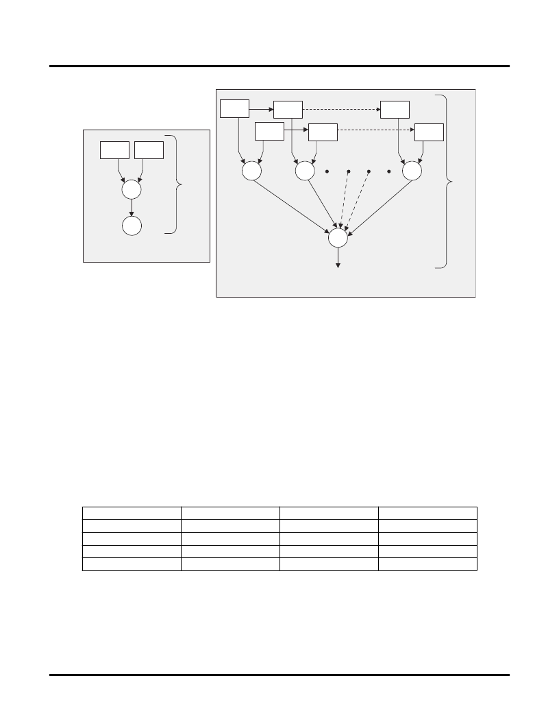
Figure 2-17. Comparison of General DSP and LatticeECP-DSP Approaches
sysDSP Block Capabilities
The sysDSP block in the LatticeECP-DSP family supports four functional elements in three 9, 18 and 36 data path
widths. The user selects a function element for a DSP block and then selects the width and type (signed/unsigned)
of its operands. The operands in the LatticeECP-DSP family sysDSP Blocks can be either signed or unsigned but
not mixed within a function element. Similarly, the operand widths cannot be mixed within a block.
The resources in each sysDSP block can be con
fi
gured to support the following four elements:
MULT
MAC
MULTADD
MULTADDSUM (Multiply, Addition/Subtraction, Accumulate)
(Multiply)
(Multiply, Accumulate)
(Multiply, Addition/Subtraction)
The number of elements available in each block depends in the width selected from the three available options x9,
x18, and x36. A number of these elements are concatenated for highly parallel implementations of DSP functions.
Table 2-1 shows the capabilities of the block.
Table 2-7. Maximum Number of Elements in a Block
Some options are available in four elements. The input register in all the elements can be directly loaded or can be
loaded as shift register from previous operand registers. In addition by selecting ‘dynamic operation’ in the ‘Signed/
Unsigned’ options the operands can be switched between signed and unsigned on every cycle. Similarly by select-
ing ‘Dynamic operation’ in the ‘Add/Sub’ option the Accumulator can be switched between addition and subtraction
on every cycle.
Width of Multiply
MULT
MAC
MULTADD
MULTADDSUM
x9
8
4
4
2
x18
4
2
2
1
x36
1
—
—
—
Multiplier 0
Operand
A
Operand
B
Operand
A
Operand
B
Operand
A
Operand
B
Multiplier 1
Multiplier
(k-1)
Accumulator
Output
m/k
loops
Single
Multiplier
x
x
x
x
Operand
A
Accumulator
Operand
B
M loops
Function implemented in
General purpose DSP
Function implemented
in LatticeECP
Σ
Σ
相關(guān)PDF資料 |
PDF描述 |
|---|---|
| LFEC33E-3F672I | LatticeECP/EC Family Data Sheet |
| LFECP33E-3F672I | LatticeECP/EC Family Data Sheet |
| LFEC33E-3F900C | LatticeECP/EC Family Data Sheet |
| LFECP33E-3F900C | LatticeECP/EC Family Data Sheet |
| LFEC33E-3F900I | LatticeECP/EC Family Data Sheet |
相關(guān)代理商/技術(shù)參數(shù) |
參數(shù)描述 |
|---|---|
| LFECP33E-3F672I | 功能描述:FPGA - 現(xiàn)場(chǎng)可編程門陣列 32.8K LUTs 496 I/O RoHS:否 制造商:Altera Corporation 系列:Cyclone V E 柵極數(shù)量: 邏輯塊數(shù)量:943 內(nèi)嵌式塊RAM - EBR:1956 kbit 輸入/輸出端數(shù)量:128 最大工作頻率:800 MHz 工作電源電壓:1.1 V 最大工作溫度:+ 70 C 安裝風(fēng)格:SMD/SMT 封裝 / 箱體:FBGA-256 |
| LFECP33E-3F900C | 制造商:LATTICE 制造商全稱:Lattice Semiconductor 功能描述:LatticeECP/EC Family Data Sheet |
| LFECP33E-3F900I | 制造商:LATTICE 制造商全稱:Lattice Semiconductor 功能描述:LatticeECP/EC Family Data Sheet |
| LFECP33E-3FN256C | 制造商:LATTICE 制造商全稱:Lattice Semiconductor 功能描述:LatticeECP/EC Family Data Sheet |
| LFECP33E-3FN256I | 制造商:LATTICE 制造商全稱:Lattice Semiconductor 功能描述:LatticeECP/EC Family Data Sheet |
發(fā)布緊急采購,3分鐘左右您將得到回復(fù)。