- 您現在的位置:買賣IC網 > PDF目錄377626 > LFEC1E-4T100C (LATTICE SEMICONDUCTOR CORP) LatticeECP/EC Family Data Sheet PDF資料下載
參數資料
| 型號: | LFEC1E-4T100C |
| 廠商: | LATTICE SEMICONDUCTOR CORP |
| 元件分類: | FPGA |
| 英文描述: | LatticeECP/EC Family Data Sheet |
| 中文描述: | FPGA, 192 CLBS, 1500 GATES, 420 MHz, PQFP100 |
| 封裝: | 14 X 14 MM, TQFP-100 |
| 文件頁數: | 20/117頁 |
| 文件大?。?/td> | 557K |
| 代理商: | LFEC1E-4T100C |
第1頁第2頁第3頁第4頁第5頁第6頁第7頁第8頁第9頁第10頁第11頁第12頁第13頁第14頁第15頁第16頁第17頁第18頁第19頁當前第20頁第21頁第22頁第23頁第24頁第25頁第26頁第27頁第28頁第29頁第30頁第31頁第32頁第33頁第34頁第35頁第36頁第37頁第38頁第39頁第40頁第41頁第42頁第43頁第44頁第45頁第46頁第47頁第48頁第49頁第50頁第51頁第52頁第53頁第54頁第55頁第56頁第57頁第58頁第59頁第60頁第61頁第62頁第63頁第64頁第65頁第66頁第67頁第68頁第69頁第70頁第71頁第72頁第73頁第74頁第75頁第76頁第77頁第78頁第79頁第80頁第81頁第82頁第83頁第84頁第85頁第86頁第87頁第88頁第89頁第90頁第91頁第92頁第93頁第94頁第95頁第96頁第97頁第98頁第99頁第100頁第101頁第102頁第103頁第104頁第105頁第106頁第107頁第108頁第109頁第110頁第111頁第112頁第113頁第114頁第115頁第116頁第117頁
2-17
Architecture
Lattice Semiconductor
LatticeECP/EC Family Data Sheet
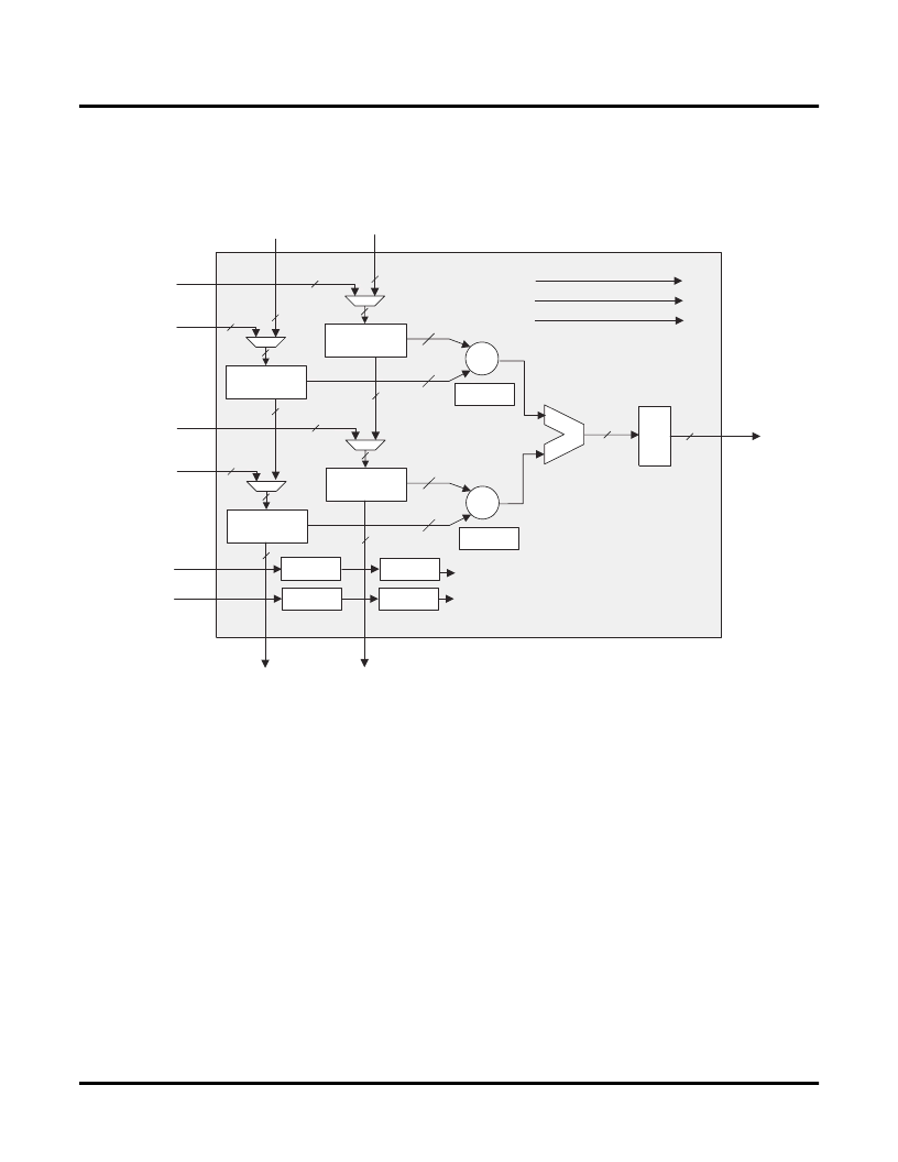
MULTADD sysDSP Element
In this case, the operands A0 and B0 are multiplied and the result is added/subtracted with the result of the multi-
plier operation of operands A1 and A2. The user can enable the input, output and pipeline registers. Figure 2-20
shows the MULTADD sysDSP element.
Figure 2-20. MULTADD
MULTADDSUM sysDSP Element
In this case, the operands A0 and B0 are multiplied and the result is added/subtracted with the result of the multi-
plier operation of operands A1 and B1. Additionally the operands A2 and B2 are multiplied and the result is added/
subtracted with the result of the multiplier operation of operands A3 and B3. The result of both addition/subtraction
are added in a summation block. The user can enable the input, output and pipeline registers. Figure 2-21 shows
the MULTADDSUM sysDSP element.
Multiplier
x
Multiplier
x
Add/Sub
n
m
m
n
m
n
m
n
n
m
m+n
(default)
m+n+1
(default)
m+n+1
(default)
m+n
(default)
n
m
m
n
m
n
n
m
Multiplier B0
Multiplicand A0
Multiplier B1
Multiplicand A1
Signed
Shift Register A In
Shift Register B In
Shift Register A Out
Shift Register B Out
Output
Addn
PiPipe
ReReg
CLK (CLK0,CLK1,CLK2,CLK3)
CE (CE0,CE1,CE2,CE3)
RST(RST0,RST1,RST2,RST3)
Input
Register
Pipeline
Register
Input
Register
Pipeline
Register
Pipeline
Register
Input Data
Register A
Input Data
Register A
Input Data
Register B
Input Data
Register B
O
R
To Add/Sub
To Add/Sub
相關PDF資料 |
PDF描述 |
|---|---|
| LFEC1E-5F672C | LatticeECP/EC Family Data Sheet |
| LFECP1E-5F672C | LatticeECP/EC Family Data Sheet |
| LFEC3E-5F672C | LatticeECP/EC Family Data Sheet |
| LFECP3E-5F672C | LatticeECP/EC Family Data Sheet |
| LFEC6E-5F672C | LatticeECP/EC Family Data Sheet |
相關代理商/技術參數 |
參數描述 |
|---|---|
| LFEC1E-4T100CES | 功能描述:FPGA - 現場可編程門陣列 1.5 LUT 67 I/O RoHS:否 制造商:Altera Corporation 系列:Cyclone V E 柵極數量: 邏輯塊數量:943 內嵌式塊RAM - EBR:1956 kbit 輸入/輸出端數量:128 最大工作頻率:800 MHz 工作電源電壓:1.1 V 最大工作溫度:+ 70 C 安裝風格:SMD/SMT 封裝 / 箱體:FBGA-256 |
| LFEC1E-4T100I | 功能描述:FPGA - 現場可編程門陣列 1.5K LUTs 67 IO 1.2V -4 Spd I RoHS:否 制造商:Altera Corporation 系列:Cyclone V E 柵極數量: 邏輯塊數量:943 內嵌式塊RAM - EBR:1956 kbit 輸入/輸出端數量:128 最大工作頻率:800 MHz 工作電源電壓:1.1 V 最大工作溫度:+ 70 C 安裝風格:SMD/SMT 封裝 / 箱體:FBGA-256 |
| LFEC1E-4T100IES | 功能描述:FPGA - 現場可編程門陣列 1.5 LUT 67 I/O RoHS:否 制造商:Altera Corporation 系列:Cyclone V E 柵極數量: 邏輯塊數量:943 內嵌式塊RAM - EBR:1956 kbit 輸入/輸出端數量:128 最大工作頻率:800 MHz 工作電源電壓:1.1 V 最大工作溫度:+ 70 C 安裝風格:SMD/SMT 封裝 / 箱體:FBGA-256 |
| LFEC1E-4T144C | 功能描述:FPGA - 現場可編程門陣列 1.5K LUTs RoHS:否 制造商:Altera Corporation 系列:Cyclone V E 柵極數量: 邏輯塊數量:943 內嵌式塊RAM - EBR:1956 kbit 輸入/輸出端數量:128 最大工作頻率:800 MHz 工作電源電壓:1.1 V 最大工作溫度:+ 70 C 安裝風格:SMD/SMT 封裝 / 箱體:FBGA-256 |
| LFEC1E-4T144CES | 功能描述:FPGA - 現場可編程門陣列 1.5 LUT 97 I/O RoHS:否 制造商:Altera Corporation 系列:Cyclone V E 柵極數量: 邏輯塊數量:943 內嵌式塊RAM - EBR:1956 kbit 輸入/輸出端數量:128 最大工作頻率:800 MHz 工作電源電壓:1.1 V 最大工作溫度:+ 70 C 安裝風格:SMD/SMT 封裝 / 箱體:FBGA-256 |
發(fā)布緊急采購,3分鐘左右您將得到回復。