- 您現(xiàn)在的位置:買賣IC網 > PDF目錄377631 > LFEC10E-4T144I (Lattice Semiconductor Corporation) RS-S_D(Z) Series - Econoline Regulated DC-DC Converters; Input Voltage (Vdc): 48V; Output Voltage (Vdc): 3.3V; Power: 2W; 2:1 and 4:1 Wide Input Voltage Ranges; 1kVDC, 2kVD & 3kVDC Isolation; UL94V-0 Package Material; Continuous Short Circuit Protection; Low Noise; No External Capacitor needed; Efficiency to 83% PDF資料下載
參數(shù)資料
| 型號: | LFEC10E-4T144I |
| 廠商: | Lattice Semiconductor Corporation |
| 元件分類: | DC/DC變換器 |
| 英文描述: | RS-S_D(Z) Series - Econoline Regulated DC-DC Converters; Input Voltage (Vdc): 48V; Output Voltage (Vdc): 3.3V; Power: 2W; 2:1 and 4:1 Wide Input Voltage Ranges; 1kVDC, 2kVD & 3kVDC Isolation; UL94V-0 Package Material; Continuous Short Circuit Protection; Low Noise; No External Capacitor needed; Efficiency to 83% |
| 中文描述: | LatticeECP / EC的系列數(shù)據(jù)手冊 |
| 文件頁數(shù): | 25/117頁 |
| 文件大小: | 557K |
| 代理商: | LFEC10E-4T144I |
第1頁第2頁第3頁第4頁第5頁第6頁第7頁第8頁第9頁第10頁第11頁第12頁第13頁第14頁第15頁第16頁第17頁第18頁第19頁第20頁第21頁第22頁第23頁第24頁當前第25頁第26頁第27頁第28頁第29頁第30頁第31頁第32頁第33頁第34頁第35頁第36頁第37頁第38頁第39頁第40頁第41頁第42頁第43頁第44頁第45頁第46頁第47頁第48頁第49頁第50頁第51頁第52頁第53頁第54頁第55頁第56頁第57頁第58頁第59頁第60頁第61頁第62頁第63頁第64頁第65頁第66頁第67頁第68頁第69頁第70頁第71頁第72頁第73頁第74頁第75頁第76頁第77頁第78頁第79頁第80頁第81頁第82頁第83頁第84頁第85頁第86頁第87頁第88頁第89頁第90頁第91頁第92頁第93頁第94頁第95頁第96頁第97頁第98頁第99頁第100頁第101頁第102頁第103頁第104頁第105頁第106頁第107頁第108頁第109頁第110頁第111頁第112頁第113頁第114頁第115頁第116頁第117頁
2-22
Architecture
Lattice Semiconductor
LatticeECP/EC Family Data Sheet
Table 2-12. PIO Signal List
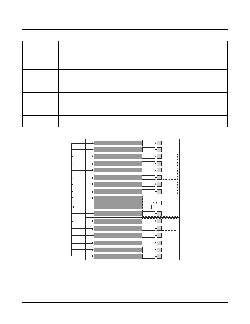
Figure 2-24. DQS Routing
PIO
The PIO contains four blocks: an input register block, output register block, tristate register block and a control logic
block. These blocks contain registers for both single data rate (SDR) and double data rate (DDR) operation along
with the necessary clock and selection logic. Programmable delay lines used to shift incoming clock and data sig-
nals are also included in these blocks.
Name
Type
Description
CE0, CE1
CLK0, CLK1
LSR
GSRN
INCK
DQS
INDD
INFF
IPOS0, IPOS1
ONEG0
OPOS0,
OPOS1 ONEG1
TD
DDRCLKPOL
Control from the core
Control from the core
Control from the core
Control from routing
Input to the core
Input to PIO
Input to the core
Input to the core
Input to the core
Control from the core
Control from the core
Tristate control from the core
Tristate control from the core
Control from clock polarity bus
Clock enables for input and output block FFs.
System clocks for input and output blocks.
Local Set/Reset.
Global Set/Reset (active low).
Input to Primary Clock Network or PLL reference inputs.
DQS signal from logic (routing) to PIO.
Unregistered data input to core.
Registered input on positive edge of the clock (CLK0).
DDRX registered inputs to the core.
Output signals from the core for SDR and DDR operation.
Output signals from the core for DDR operation
Signals to Tristate Register block for DDR operation.
Tristate signal from the core used in SDR operation.
Controls the polarity of the clock (CLK0) that feed the DDR input block.
PIO A
PIO B
PADA "T"
LVDS Pair
PADB "C"
PIO B
PIO A
PIO B
PIO A
Assigned
DQS Pin
PADA "T"
DQS
sysIO
Buffer
PADB "C"
LVDS Pair
PADA "T"
LVDS Pair
PADB "C"
PIO A
PIO B
PADA "T"
LVDS Pair
PADB "C"
PIO A
PIO B
PADA "T"
LVDS Pair
PADB "C"
PIO A
PIO B
PADA "T"
LVDS Pair
PADB "C"
PIO A
PIO B
PADA "T"
LVDS Pair
PADB "C"
PIO A
PIO B
PADA "T"
LVDS Pair
PADB "C"
Delay
相關PDF資料 |
PDF描述 |
|---|---|
| LFEC10E-5F256C | RS-S_D(Z) Series - Econoline Regulated DC-DC Converters; Input Voltage (Vdc): 48V; Output Voltage (Vdc): 3.3V; Power: 2W; 2:1 and 4:1 Wide Input Voltage Ranges; 1kVDC, 2kVD & 3kVDC Isolation; UL94V-0 Package Material; Continuous Short Circuit Protection; Low Noise; No External Capacitor needed; Efficiency to 83% |
| LFEC10E-5F256I | LatticeECP/EC Family Data Sheet |
| LFEC20E-3T144C | LatticeECP/EC Family Data Sheet |
| LFEC20E-3T144I | LatticeECP/EC Family Data Sheet |
| LFEC20E-4F256C | LatticeECP/EC Family Data Sheet |
相關代理商/技術參數(shù) |
參數(shù)描述 |
|---|---|
| LFEC10E-4TN100C | 制造商:LATTICE 制造商全稱:Lattice Semiconductor 功能描述:LatticeECP/EC Family Data Sheet |
| LFEC10E-4TN100I | 制造商:LATTICE 制造商全稱:Lattice Semiconductor 功能描述:LatticeECP/EC Family Data Sheet |
| LFEC10E-4TN144C | 制造商:LATTICE 制造商全稱:Lattice Semiconductor 功能描述:LatticeECP/EC Family Data Sheet |
| LFEC10E-4TN144I | 制造商:LATTICE 制造商全稱:Lattice Semiconductor 功能描述:LatticeECP/EC Family Data Sheet |
| LFEC10E-5F256C | 功能描述:FPGA - 現(xiàn)場可編程門陣列 10.2K LUTs RoHS:否 制造商:Altera Corporation 系列:Cyclone V E 柵極數(shù)量: 邏輯塊數(shù)量:943 內嵌式塊RAM - EBR:1956 kbit 輸入/輸出端數(shù)量:128 最大工作頻率:800 MHz 工作電源電壓:1.1 V 最大工作溫度:+ 70 C 安裝風格:SMD/SMT 封裝 / 箱體:FBGA-256 |
發(fā)布緊急采購,3分鐘左右您將得到回復。