- 您現(xiàn)在的位置:買賣IC網(wǎng) > PDF目錄377624 > LF3347 (Logic Devices Incorporated) High-Speed Image Filter with Coefficient RAM(高速圖像濾波器(帶系數(shù)RAM)) PDF資料下載
參數(shù)資料
| 型號(hào): | LF3347 |
| 廠商: | Logic Devices Incorporated |
| 英文描述: | High-Speed Image Filter with Coefficient RAM(高速圖像濾波器(帶系數(shù)RAM)) |
| 中文描述: | 高速圖像濾波器的系數(shù)存儲(chǔ)器(高速圖像濾波器(帶系數(shù)的RAM)) |
| 文件頁數(shù): | 4/10頁 |
| 文件大小: | 80K |
| 代理商: | LF3347 |
DEVICES INCORPORATED
LF3347
High-Speed Image Filter with Coefficient RAM
4
Video Imaging Products
08/16/2000–LDS.3347-G
FUNCTIONAL DESCRIPTION
Coefficient Banks
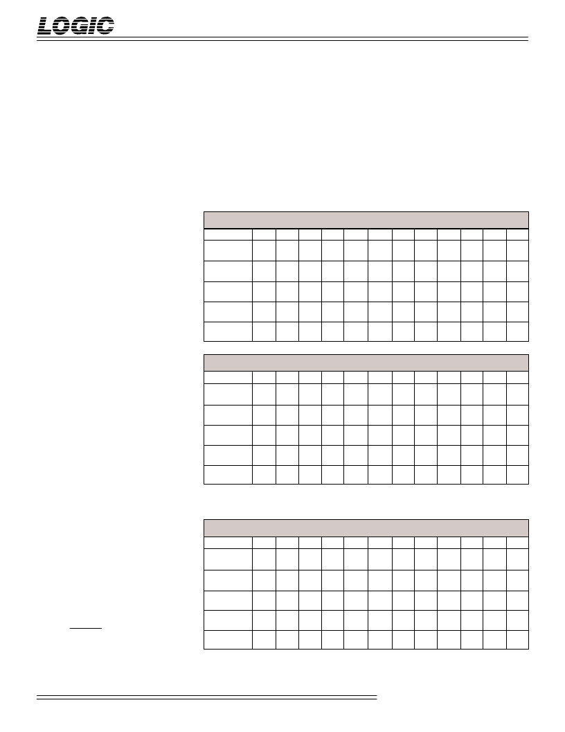
The LF3347 has four coefficient banks
which feed coefficient values to the
multipliers. Each bank can store 256
12-bit coefficients. In the example
shown in Table 3, address 10 in coeffi-
cient banks 1 through 4 is loaded with
the following values: ABCH, 789H,
456H, 123H. The coefficient banks are
not written to until all four coefficients
have been loaded into the device.
A
7-0
determines which coefficient set is
sent to the multipliers. A value of 0 on
A
7-0
selects set 0. A value of 1 selects
set 1 and so on.
Rounding/Offset
The accumulator output may be rounded
before being sent to the output select
section. Rounding is user-selectable and
is accomplished by adding the contents of
a round register to the accumulator
output (see Figure 2). There are sixteen
32-bit round registers. In the example in
Table 4, round register 10 is loaded with
76543210H. A round register is not
written to until all four data values have
been loaded into the device.
SELRND
3-0
determines which round
register is used for rounding. A value of 0
on SELRND
3-0
selects round register 0. A
value of 1 selects round register 1 and so
on. If rounding is not desired, a round
register should be loaded with 0 and
selected as the register for rounding.
Output Select
The filter output word width is 32-bits.
However, only 16-bits may be sent to the
device output. SHIFT4-0 determines
which 16 bits are passed to the device
output (See Table 1).
Output Limiting
An output limiting function is provided
for the output of the filter. When limiting is
enabled (LMTEN LOW), the limit register
selected with SELLMT
3-0
determines the
valid range of output values for the overall
filter. There are sixteen 32-bit limit
registers. Each limit register contains both
an upper and lower limit value. The
lower limit is stored in bits 15-0 and the
upper limit is stored in bits 31-16. If the
value fed to the limiting circuitry is less
than the lower limit, the lower limit is
passed to the device output. If the value
fed to the limiting circuitry is greater than
the upper limit, the upper limit is passed
to the device output. When loading limit
values into the device, the upper limit must
T
ABLE
3.
C
OEFFICIENT
B
ANK
L
OADING
F
ORMAT
CC
11
CC
10
CC
9
CC
8
CC
7
CC
6
CC
5
CC
4
CC
3
CC
2
CC
1
CC
0
0
0
0
0
0
0
1st Word
Address
2nd Word
Bank 1
3rd Word
Bank 2
4th Word
Bank 3
5th Word
Bank 4
0
0
1
0
1
0
1
0
1
0
1
0
1
1
1
1
0
0
0
1
1
1
1
0
0
0
1
0
0
1
0
1
0
0
0
1
0
1
0
1
1
0
0
0
0
1
0
0
1
0
0
0
1
1
T
ABLE
4.
R
OUND
R
EGISTER
L
OADING
F
ORMAT
CC
11
CC
10
CC
9
CC
8
CC
7
CC
6
CC
5
CC
4
CC
3
CC
2
CC
1
CC
0
1
0
0
0
0
0
1st Word
Address
2nd Word
0
0
1
0
1
0
R
R
R
R
0
0
0
1
0
0
0
*0
3rd Word
R
R
R
R
0
0
1
1
0
0
1
0
4th Word
R
R
R
R
0
1
0
1
0
1
0
0
5th Word
R
R
R
R
**0
1
1
1
0
1
1
0
T
ABLE
5.
L
IMIT
R
EGISTER
L
OADING
F
ORMAT
CC
11
CC
10
CC
9
CC
8
CC
7
CC
6
CC
5
CC
4
CC
3
CC
2
CC
1
CC
0
1
1
0
0
0
0
1st Word
Address
2nd Word
0
0
1
1
1
1
R
R
R
R
0
0
1
0
0
0
1
1
3rd Word
R
R
R
R
*0
0
0
0
0
0
0
1
4th Word
R
R
R
R
1
1
1
0
1
1
0
1
5th Word
R
R
R
R
**0
1
1
1
1
1
1
1
R = Reserved. Must be set to “0”.
* This bit represents the MSB of the Lower Limit Register.
** This bit represents the MSB of Upper Limit Register.
R = Reserved. Must be set to “0”.
* This bit represents the LSB of the Round Register.
** This bit represents the MSB of the Round Register.
be greater than the lower limit. In the
example shown in Table 4, limit register
15 is loaded with a lower limit of 0123H
and an upper limit of 7FEDH. A limit
register is not written to until all four data
values have been loaded into the device.
SELLMT
3-0
determines which limit
register is used for limiting. A value of 0
on SELLMT
3-0
selects limit register 0. A
value of 1 selects limit register 1 and so on.
相關(guān)PDF資料 |
PDF描述 |
|---|---|
| LF3347QC12 | CAP 1.0UF 63V METAL POLY |
| LF3347QC15 | High-Speed Image Filter with Coefficient RAM |
| LF3370QC12 | High-Definition Video Format Converter |
| LF3370 | High-Definition Video Format Converter(高清晰度視頻格式轉(zhuǎn)換器) |
| LF39J8 | DIODE ZENER TRIPLE ISOLATED 200mW 8.2Vz 20mA-Izt 0.05 3uA-Ir 6.5 SOT-363 3K/REEL |
相關(guān)代理商/技術(shù)參數(shù) |
參數(shù)描述 |
|---|---|
| LF3347D | 制造商:n/a 功能描述:3347 NSC'85 S8J2B |
| LF3347GC12 | 制造商:未知廠家 制造商全稱:未知廠家 功能描述:Digital Filter |
| LF3347GC15 | 制造商:未知廠家 制造商全稱:未知廠家 功能描述:Digital Filter |
| LF3347GC25 | 制造商:未知廠家 制造商全稱:未知廠家 功能描述:Digital Filter |
| LF3347GM12 | 制造商:未知廠家 制造商全稱:未知廠家 功能描述:Digital Filter |
發(fā)布緊急采購,3分鐘左右您將得到回復(fù)。