- 您現(xiàn)在的位置:買賣IC網(wǎng) > PDF目錄358761 > LC74725 (Sanyo Electric Co.,Ltd.) On-Screen Display Controller LSI PDF資料下載
參數(shù)資料
| 型號(hào): | LC74725 |
| 廠商: | Sanyo Electric Co.,Ltd. |
| 英文描述: | On-Screen Display Controller LSI |
| 中文描述: | 屏幕顯示控制器芯片 |
| 文件頁(yè)數(shù): | 8/16頁(yè) |
| 文件大小: | 260K |
| 代理商: | LC74725 |
第1頁(yè)第2頁(yè)第3頁(yè)第4頁(yè)第5頁(yè)第6頁(yè)第7頁(yè)當(dāng)前第8頁(yè)第9頁(yè)第10頁(yè)第11頁(yè)第12頁(yè)第13頁(yè)第14頁(yè)第15頁(yè)第16頁(yè)
No. 5213-8/16
LC74725, 74725M
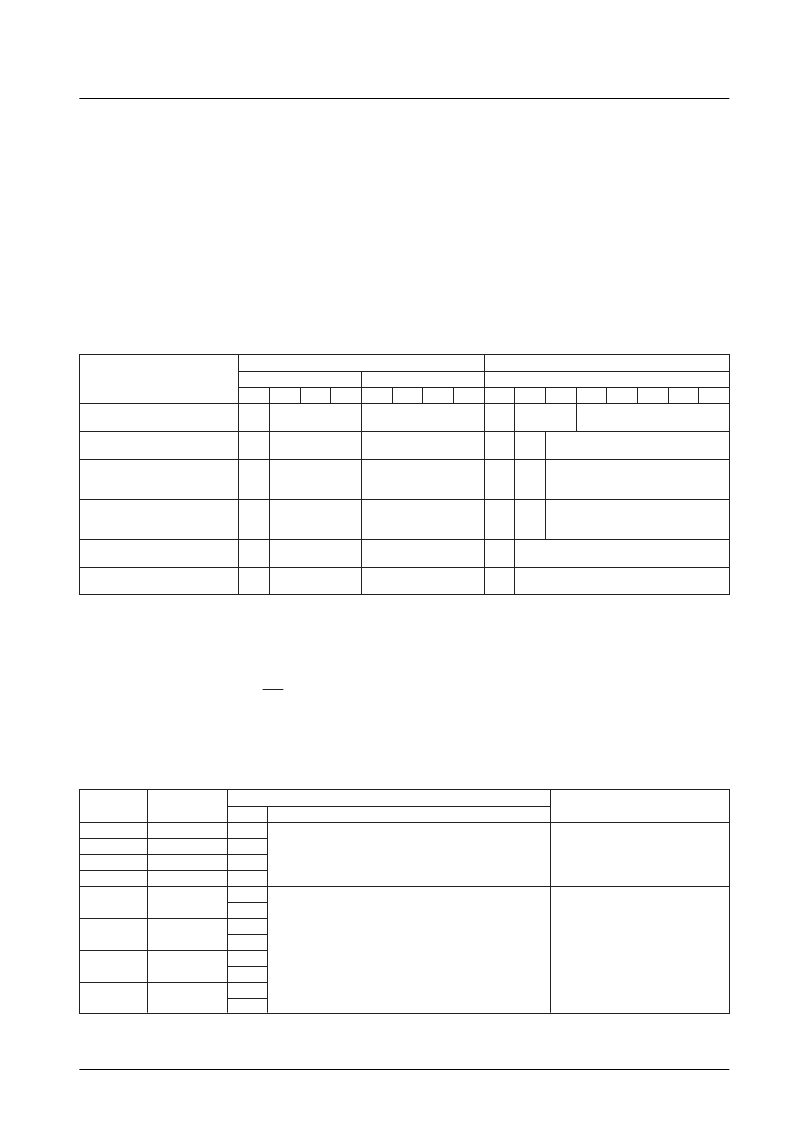
Display Control Commands
Display control commands have an 8-bit format and are transferred using the serial input function. Commands consist of
a command identification code in the first byte and command data in the following bytes. The following commands are
supported.
x
COMMAND0: Display memory (VRAM) write address setup command
y
COMMAND1: Display character data write command
z
COMMAND2: Vertical display start position and vertical character size setup command
{
COMMAND3: Horizontal display start position and horizontal character size setup command
|
COMMAND4: Display control setup command
}
COMMAND5: Display control setup command
Display Control Command Table
Once written, the command identification code in the first byte is stored until the next first byte is written. However,
when the display character data write command (COMMAND1) is written, the LC74725/M locks into the display
character data write mode, and another first byte cannot be written.
When a high level is input to the CS pin, the LC74725/M is set to COMMAND0 (display memory write address setup
mode).
x
COMMAND0 (Display memory write address setup command)
First byte
First byte
Second byte
Command
Command identification code
Data
Data
7
6
5
4
3
2
1
0
7
6
5
4
3
2
1
0
COMMAND0
Set write address
1
0
0
0
V3
V2
V1
V0
0
0
0
H4
H3
H2
H1
H0
COMMAND1
Write character
1
0
0
1
0
0
0
0
at
0
c5
c4
c3
c2
c1
c0
COMMAND2
Set vertical display start position and
vertical character size
1
0
1
0
0
VS
20
0
VS
10
0
FS
VP
5
VP
4
VP
3
VP
2
VP
1
VP
0
COMMAND3
Set horizontal display start position
and horizontal character size
1
0
1
1
EGP
HS
20
0
HS
10
0
LC
HP
5
HP
4
HP
3
HP
2
HP
1
HP
0
COMMAND4
Display control
1
1
0
0
TST
MOD
RAM
ERS
OSC
STP
SYS
RST
0
EGL
NON
EG
BK
1
BK
0
RV
DSP
ON
COMMAND5
Synchronizing signal control
1
1
0
1
BCL
PH
RSN
INT
0
0
0
MUT
MOD
0
CTL
3
CTL
2
SEL
0
Register content
DA0 to DA7
Register name
State
Function
Note
7
—
1
6
—
0
Command 0 identification code
Set the display memory write address.
5
—
0
4
—
0
3
V3
0
1
2
V2
0
1
Display memory row address (0 to 9 hexadecimal)
1
V1
0
1
0
V0
0
1
相關(guān)PDF資料 |
PDF描述 |
|---|---|
| LC74725M | On-Screen Display Controller LSI |
| LC7472 | On-screen Video Display Controller for NTSC or PAL-M |
| LC7472M | On-screen Video Display Controller for NTSC or PAL-M |
| LC74730M | On-Screen Display Controller LSI |
| LC74731 | On-Screen Display Controller |
相關(guān)代理商/技術(shù)參數(shù) |
參數(shù)描述 |
|---|---|
| LC74725M | 制造商:SANYO 制造商全稱:Sanyo Semicon Device 功能描述:On-Screen Display Controller LSI |
| LC7472M | 制造商:SANYO 制造商全稱:Sanyo Semicon Device 功能描述:On-screen Video Display Controller for NTSC or PAL-M |
| LC7472NM9048 | 制造商:Panasonic Industrial Company 功能描述:IC |
| LC7472NM9056 | 制造商:Panasonic Industrial Company 功能描述:IC |
| LC74730M | 制造商:SANYO 制造商全稱:Sanyo Semicon Device 功能描述:On-Screen Display Controller LSI |
發(fā)布緊急采購(gòu),3分鐘左右您將得到回復(fù)。