- 您現(xiàn)在的位置:買賣IC網(wǎng) > PDF目錄377609 > LC4512Z (Lattice Semiconductor Corporation) 3.3V/2.5V/1.8V In-System Programmable SuperFAST High density PDLs PDF資料下載
參數(shù)資料
| 型號(hào): | LC4512Z |
| 廠商: | Lattice Semiconductor Corporation |
| 英文描述: | 3.3V/2.5V/1.8V In-System Programmable SuperFAST High density PDLs |
| 中文描述: | 3.3V/2.5V/1.8V在系統(tǒng)可編程超快高密度PDLs |
| 文件頁(yè)數(shù): | 27/91頁(yè) |
| 文件大小: | 851K |
| 代理商: | LC4512Z |
第1頁(yè)第2頁(yè)第3頁(yè)第4頁(yè)第5頁(yè)第6頁(yè)第7頁(yè)第8頁(yè)第9頁(yè)第10頁(yè)第11頁(yè)第12頁(yè)第13頁(yè)第14頁(yè)第15頁(yè)第16頁(yè)第17頁(yè)第18頁(yè)第19頁(yè)第20頁(yè)第21頁(yè)第22頁(yè)第23頁(yè)第24頁(yè)第25頁(yè)第26頁(yè)當(dāng)前第27頁(yè)第28頁(yè)第29頁(yè)第30頁(yè)第31頁(yè)第32頁(yè)第33頁(yè)第34頁(yè)第35頁(yè)第36頁(yè)第37頁(yè)第38頁(yè)第39頁(yè)第40頁(yè)第41頁(yè)第42頁(yè)第43頁(yè)第44頁(yè)第45頁(yè)第46頁(yè)第47頁(yè)第48頁(yè)第49頁(yè)第50頁(yè)第51頁(yè)第52頁(yè)第53頁(yè)第54頁(yè)第55頁(yè)第56頁(yè)第57頁(yè)第58頁(yè)第59頁(yè)第60頁(yè)第61頁(yè)第62頁(yè)第63頁(yè)第64頁(yè)第65頁(yè)第66頁(yè)第67頁(yè)第68頁(yè)第69頁(yè)第70頁(yè)第71頁(yè)第72頁(yè)第73頁(yè)第74頁(yè)第75頁(yè)第76頁(yè)第77頁(yè)第78頁(yè)第79頁(yè)第80頁(yè)第81頁(yè)第82頁(yè)第83頁(yè)第84頁(yè)第85頁(yè)第86頁(yè)第87頁(yè)第88頁(yè)第89頁(yè)第90頁(yè)第91頁(yè)
Lattice Semiconductor
ispMACH 4000V/B/C/Z Family Data Sheet
27
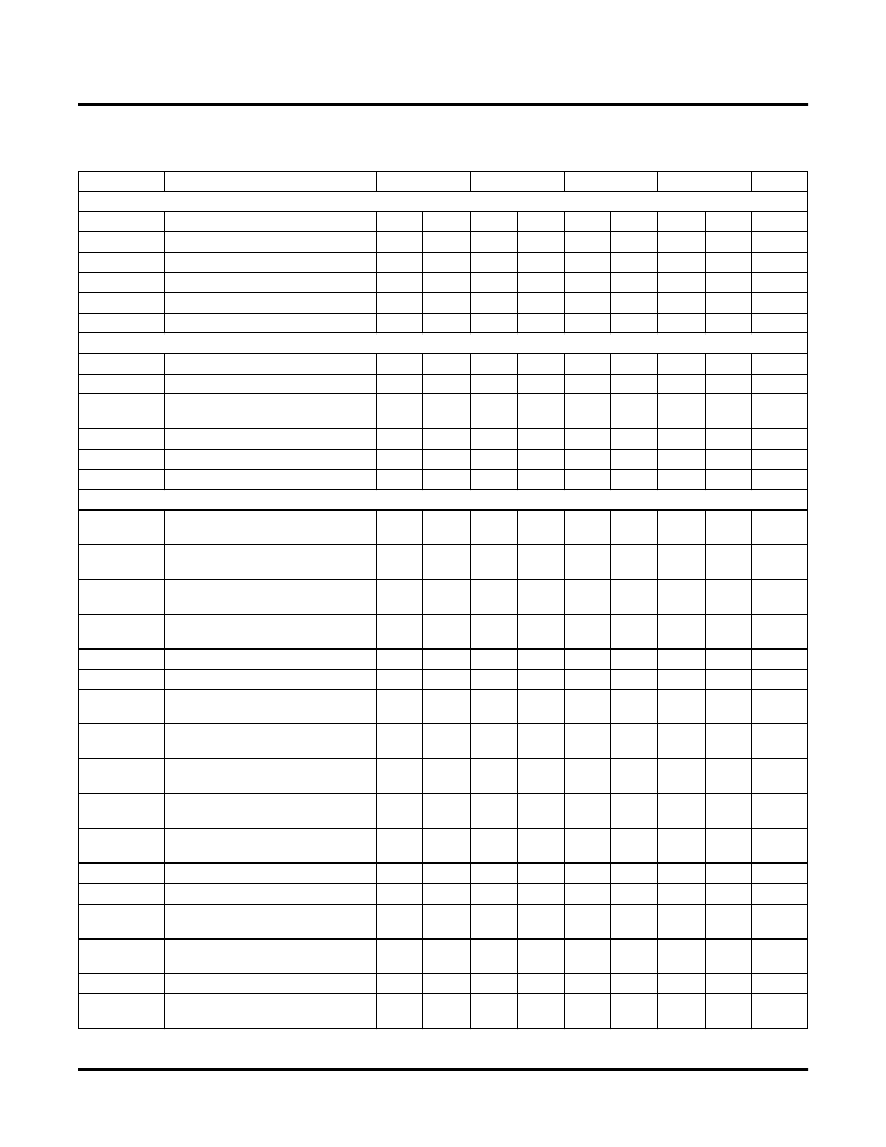
ispMACH 4000V/B/C Internal Timing Parameters
Over Recommended Operating Conditions
Parameter
Description
-2.5
-2.7
-3
-3.5
Units
In/Out Delays
t
IN
t
GOE
t
GCLK_IN
t
BUF
t
EN
t
DIS
Routing/GLB Delays
Input Buffer Delay
—
0.60
—
0.60
—
0.70
—
0.70
ns
Global OE Pin Delay
—
2.04
—
2.54
—
3.04
—
3.54
ns
Global Clock Input Buffer Delay
—
0.78
—
1.28
—
1.28
—
1.28
ns
Delay through Output Buffer
—
0.85
—
0.85
—
0.85
—
0.85
ns
Output Enable Time
—
0.96
—
0.96
—
0.96
—
0.96
ns
Output Disable Time
—
0.96
—
0.96
—
0.96
—
0.96
ns
t
ROUTE
t
MCELL
Delay through GRP
—
0.61
—
0.81
—
1.01
—
1.01
ns
Macrocell Delay
—
0.45
—
0.55
—
0.55
—
0.65
ns
t
INREG
Input Buffer to Macrocell Register
Delay
—
0.11
—
0.31
—
0.31
—
0.31
ns
t
FBK
t
PDb
t
PDi
Register/Latch Delays
Internal Feedback Delay
—
0.00
—
0.00
—
0.00
—
0.00
ns
5-PT Bypass Propagation Delay
—
0.44
—
0.44
—
0.44
—
0.94
ns
Macrocell Propagation Delay
—
0.64
—
0.64
—
0.64
—
0.94
ns
t
S
D-Register Setup Time
(Global Clock)
0.92
—
1.12
—
1.02
—
0.92
—
ns
t
S_PT
D-Register Setup Time
(Product Term Clock)
1.42
—
1.32
—
1.32
—
1.32
—
ns
t
ST
T-Register Setup Time
(Global Clock)
1.12
—
1.32
—
1.22
—
1.12
—
ns
t
ST_PT
T-Register Setup Time
(Product Term Clock)
1.42
—
1.32
—
1.32
—
1.32
—
ns
t
H
t
HT
D-Register Hold Time
0.88
—
0.68
—
0.98
—
1.08
—
ns
T-Register Hold Time
0.88
—
0.68
—
0.98
—
1.08
—
ns
t
SIR
D-Input Register Setup Time
(Global Clock)
0.82
—
1.37
—
1.27
—
1.27
—
ns
t
SIR_PT
D-Input Register Setup Time
(Product Term Clock)
1.45
—
1.45
—
1.45
—
1.45
—
ns
t
HIR
D-Input Register Hold Time
(Global Clock)
0.88
—
0.63
—
0.73
—
0.73
—
ns
t
HIR_PT
D-Input Register Hold Time
(Product Term Clock)
0.88
—
0.63
—
0.73
—
0.73
—
ns
t
COi
Register Clock to Output/Feedback
MUX Time
—
0.52
—
0.52
—
0.52
—
0.52
ns
t
CES
t
CEH
Clock Enable Setup Time
2.25
—
2.25
—
2.25
—
2.25
—
ns
Clock Enable Hold Time
1.88
—
1.88
—
1.88
—
1.88
—
ns
t
SL
Latch Setup Time
(Global Clock)
0.92
—
1.12
—
1.02
—
0.92
—
ns
t
SL_PT
Latch Setup Time (Product Term
Clock)
1.42
—
1.32
—
1.32
—
1.32
—
ns
t
HL
Latch Hold Time
1.17
—
1.17
—
1.17
—
1.17
—
ns
t
GOi
Latch Gate to Output/Feedback
MUX Time
—
0.33
—
0.33
—
0.33
—
0.33
ns
相關(guān)PDF資料 |
PDF描述 |
|---|---|
| LC4128ZC-42M132C1 | 3.3V/2.5V/1.8V In-System Programmable SuperFAST High density PDLs |
| LC4128ZC-42T100C | 3.3V/2.5V/1.8V In-System Programmable SuperFAST High density PDLs |
| LC4128ZC-75M132C1 | 3.3V/2.5V/1.8V In-System Programmable SuperFAST High density PDLs |
| LC4128ZC-75T100C | 3.3V/2.5V/1.8V In-System Programmable SuperFAST High density PDLs |
| LC4032ZC-75T48I | 3.3V/2.5V/1.8V In-System Programmable SuperFAST High density PDLs |
相關(guān)代理商/技術(shù)參數(shù) |
參數(shù)描述 |
|---|---|
| LC451-6-BL | 制造商:Carling Technologies 功能描述:L SLIDE SWITCH - Bulk |
| LC4528B | 制造商:未知廠家 制造商全稱:未知廠家 功能描述:Logic IC |
| LC4536C | 制造商:INT 功能描述:120-277VV |
| LC4584B | 制造商:未知廠家 制造商全稱:未知廠家 功能描述:Logic IC |
| LC45A | 制造商:Microsemi Corporation 功能描述:TVS SGL UNI-DIR 45V 1.5KW 2PIN DO-13 - Bulk |
發(fā)布緊急采購(gòu),3分鐘左右您將得到回復(fù)。