- 您現(xiàn)在的位置:買賣IC網(wǎng) > PDF目錄377609 > LC4512Z (Lattice Semiconductor Corporation) 3.3V/2.5V/1.8V In-System Programmable SuperFAST High density PDLs PDF資料下載
參數(shù)資料
| 型號: | LC4512Z |
| 廠商: | Lattice Semiconductor Corporation |
| 英文描述: | 3.3V/2.5V/1.8V In-System Programmable SuperFAST High density PDLs |
| 中文描述: | 3.3V/2.5V/1.8V在系統(tǒng)可編程超快高密度PDLs |
| 文件頁數(shù): | 23/91頁 |
| 文件大小: | 851K |
| 代理商: | LC4512Z |
第1頁第2頁第3頁第4頁第5頁第6頁第7頁第8頁第9頁第10頁第11頁第12頁第13頁第14頁第15頁第16頁第17頁第18頁第19頁第20頁第21頁第22頁當(dāng)前第23頁第24頁第25頁第26頁第27頁第28頁第29頁第30頁第31頁第32頁第33頁第34頁第35頁第36頁第37頁第38頁第39頁第40頁第41頁第42頁第43頁第44頁第45頁第46頁第47頁第48頁第49頁第50頁第51頁第52頁第53頁第54頁第55頁第56頁第57頁第58頁第59頁第60頁第61頁第62頁第63頁第64頁第65頁第66頁第67頁第68頁第69頁第70頁第71頁第72頁第73頁第74頁第75頁第76頁第77頁第78頁第79頁第80頁第81頁第82頁第83頁第84頁第85頁第86頁第87頁第88頁第89頁第90頁第91頁
Lattice Semiconductor
ispMACH 4000V/B/C/Z Family Data Sheet
23
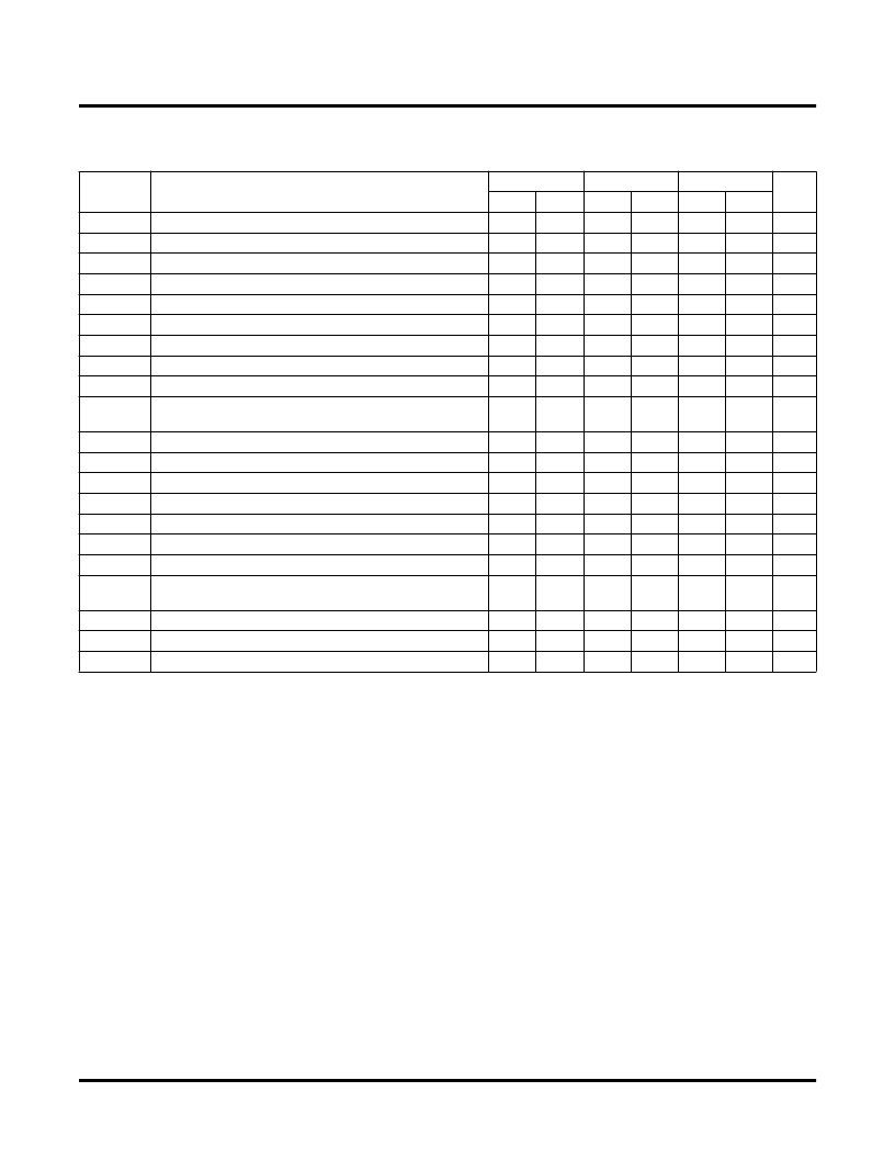
ispMACH 4000V/B/C External Switching Characteristics (Cont.)
Over Recommended Operating Conditions
Parameter
Description
1, 2, 3
-5
-75
-10
Units
Min.
Max.
Min.
Max.
Min.
Max.
t
PD
t
PD_MC
t
S
t
ST
t
SIR
t
SIRZ
t
H
t
HT
t
HIR
5-PT bypass combinatorial propagation delay
—
5.0
—
7.5
—
10.0
ns
20-PT combinatorial propagation delay through macrocell
—
5.5
—
8.0
—
10.5
ns
GLB register setup time before clock
3.0
—
4.5
—
5.5
—
ns
GLB register setup time before clock with T-type register
3.2
—
4.7
—
5.5
—
ns
GLB register setup time before clock, input register path
1.2
—
1.7
—
1.7
—
ns
GLB register setup time before clock with zero hold
2.2
—
2.7
—
2.7
—
ns
GLB register hold time after clock
0.0
—
0.0
—
0.0
—
ns
GLB register hold time after clock with T-type register
0.0
—
0.0
—
0.0
—
ns
GLB register hold time after clock, input register path
1.0
—
1.0
—
1.0
—
ns
t
HIRZ
GLB register hold time after clock, input register path with
zero hold
0.0
—
0.0
—
0.0
—
ns
t
CO
t
R
t
RW
t
PTOE/DIS
t
GPTOE/DIS
t
GOE/DIS
t
CW
GLB register clock-to-output delay
—
3.4
—
4.5
—
6.0
ns
External reset pin to output delay
—
6.3
—
9.0
—
10.5
ns
External reset pulse duration
2.0
—
4.0
—
4.0
—
ns
Input to output local product term output enable/disable
—
7.0
—
9.0
—
10.5
ns
Input to output global product term output enable/disable
—
9.0
—
10.3
—
12.0
ns
Global OE input to output enable/disable
—
5.0
—
7.0
—
8.0
ns
Global clock width, high or low
2.2
—
3.3
—
4.0
—
ns
t
GW
Global gate width low (for low transparent) or high (for
high transparent)
2.2
—
3.3
—
4.0
—
ns
t
WIR
f
MAX
f
MAX
(Ext.) Clock frequency with external feedback, [1/ (t
S
+ t
CO
)]
1. Timing numbers are based on default LVCMOS 1.8 I/O buffers. Use timing adjusters provided to calculate other standards.
2. Measured using standard switching circuit, assuming GRP loading of 1 and 1 output switching.
3. Pulse widths and clock widths less than minimum will cause unknown behavior.
4. Standard 16-bit counter using GRP feedback.
Input register clock width, high or low
2.2
—
3.3
—
4.0
—
ns
4
Clock frequency with internal feedback
227
—
168
—
125
—
MHz
156
—
111
—
86
—
MHz
Timing v.3.2
相關(guān)PDF資料 |
PDF描述 |
|---|---|
| LC4128ZC-42M132C1 | 3.3V/2.5V/1.8V In-System Programmable SuperFAST High density PDLs |
| LC4128ZC-42T100C | 3.3V/2.5V/1.8V In-System Programmable SuperFAST High density PDLs |
| LC4128ZC-75M132C1 | 3.3V/2.5V/1.8V In-System Programmable SuperFAST High density PDLs |
| LC4128ZC-75T100C | 3.3V/2.5V/1.8V In-System Programmable SuperFAST High density PDLs |
| LC4032ZC-75T48I | 3.3V/2.5V/1.8V In-System Programmable SuperFAST High density PDLs |
相關(guān)代理商/技術(shù)參數(shù) |
參數(shù)描述 |
|---|---|
| LC451-6-BL | 制造商:Carling Technologies 功能描述:L SLIDE SWITCH - Bulk |
| LC4528B | 制造商:未知廠家 制造商全稱:未知廠家 功能描述:Logic IC |
| LC4536C | 制造商:INT 功能描述:120-277VV |
| LC4584B | 制造商:未知廠家 制造商全稱:未知廠家 功能描述:Logic IC |
| LC45A | 制造商:Microsemi Corporation 功能描述:TVS SGL UNI-DIR 45V 1.5KW 2PIN DO-13 - Bulk |
發(fā)布緊急采購,3分鐘左右您將得到回復(fù)。