- 您現(xiàn)在的位置:買(mǎi)賣(mài)IC網(wǎng) > PDF目錄377609 > LC4000C (Lattice Semiconductor Corporation) 3.3V/2.5V/1.8V In-System Programmable SuperFAST High density PDLs PDF資料下載
參數(shù)資料
| 型號(hào): | LC4000C |
| 廠商: | Lattice Semiconductor Corporation |
| 英文描述: | 3.3V/2.5V/1.8V In-System Programmable SuperFAST High density PDLs |
| 中文描述: | 3.3V/2.5V/1.8V在系統(tǒng)可編程超快高密度PDLs |
| 文件頁(yè)數(shù): | 8/91頁(yè) |
| 文件大?。?/td> | 851K |
| 代理商: | LC4000C |
第1頁(yè)第2頁(yè)第3頁(yè)第4頁(yè)第5頁(yè)第6頁(yè)第7頁(yè)當(dāng)前第8頁(yè)第9頁(yè)第10頁(yè)第11頁(yè)第12頁(yè)第13頁(yè)第14頁(yè)第15頁(yè)第16頁(yè)第17頁(yè)第18頁(yè)第19頁(yè)第20頁(yè)第21頁(yè)第22頁(yè)第23頁(yè)第24頁(yè)第25頁(yè)第26頁(yè)第27頁(yè)第28頁(yè)第29頁(yè)第30頁(yè)第31頁(yè)第32頁(yè)第33頁(yè)第34頁(yè)第35頁(yè)第36頁(yè)第37頁(yè)第38頁(yè)第39頁(yè)第40頁(yè)第41頁(yè)第42頁(yè)第43頁(yè)第44頁(yè)第45頁(yè)第46頁(yè)第47頁(yè)第48頁(yè)第49頁(yè)第50頁(yè)第51頁(yè)第52頁(yè)第53頁(yè)第54頁(yè)第55頁(yè)第56頁(yè)第57頁(yè)第58頁(yè)第59頁(yè)第60頁(yè)第61頁(yè)第62頁(yè)第63頁(yè)第64頁(yè)第65頁(yè)第66頁(yè)第67頁(yè)第68頁(yè)第69頁(yè)第70頁(yè)第71頁(yè)第72頁(yè)第73頁(yè)第74頁(yè)第75頁(yè)第76頁(yè)第77頁(yè)第78頁(yè)第79頁(yè)第80頁(yè)第81頁(yè)第82頁(yè)第83頁(yè)第84頁(yè)第85頁(yè)第86頁(yè)第87頁(yè)第88頁(yè)第89頁(yè)第90頁(yè)第91頁(yè)
Lattice Semiconductor
ispMACH 4000V/B/C/Z Family Data Sheet
8
Block CLK2
Block CLK3
PT Clock
PT Clock Inverted
Shared PT Clock
Ground
Clock Enable Multiplexer
Each macrocell has a 4:1 clock enable multiplexer. This allows the clock enable signal to be selected from the fol-
lowing four sources:
PT Initialization/CE
PT Initialization/CE Inverted
Shared PT Clock
Logic High
Initialization Control
The ispMACH 4000 family architecture accommodates both block-level and macrocell-level set and reset capability.
There is one block-level initialization term that is distributed to all macrocell registers in a GLB. At the macrocell
level, two product terms can be “stolen” from the cluster associated with a macrocell to be used for set/reset func-
tionality. A reset/preset swapping feature in each macrocell allows for reset and preset to be exchanged, providing
fl
exibility.
Note that the reset/preset swapping selection feature affects power-up reset as well. All
fl
ip-
fl
ops power up to a
known state for predictable system initialization. If a macrocell is con
fi
gured to SET on a signal from the block-level
initialization, then that macrocell will be SET during device power-up. If a macrocell is con
fi
gured to RESET on a
signal from the block-level initialization or is not con
fi
gured for set/reset, then that macrocell will RESET on power-
up. To guarantee initialization values, the V
CC
rise must be monotonic, and the clock must be inactive until the reset
delay time has elapsed.
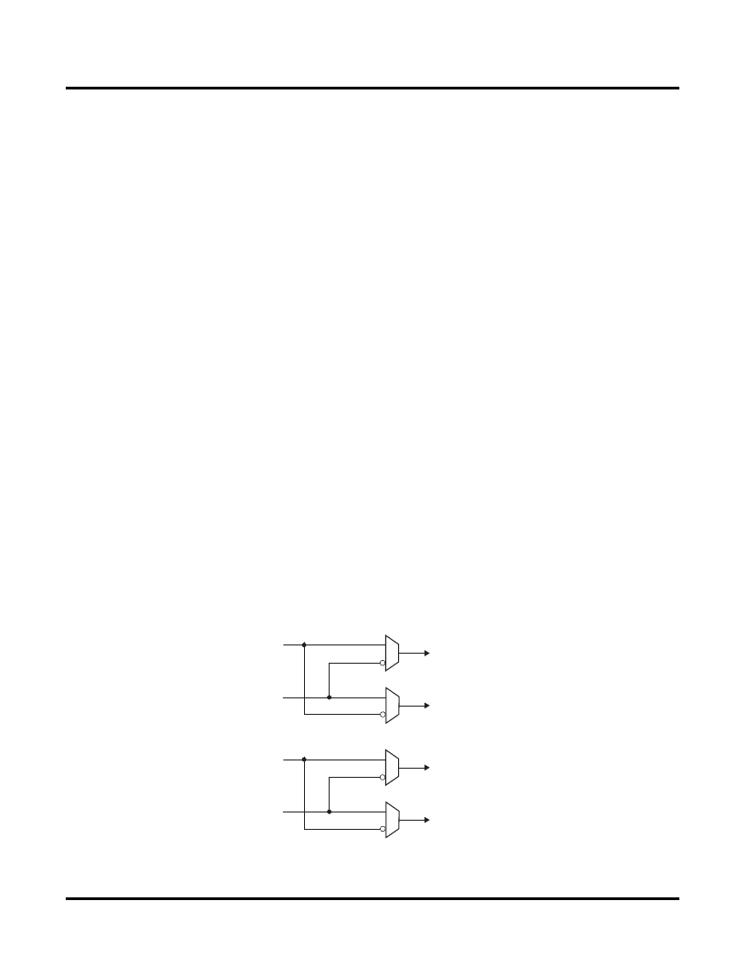
GLB Clock Generator
Each ispMACH 4000 device has up to four clock pins that are also routed to the GRP to be used as inputs. These
pins drive a clock generator in each GLB, as shown in Figure 6. The clock generator provides four clock signals that
can be used anywhere in the GLB. These four GLB clock signals can consist of a number of combinations of the
true and complement edges of the global clock signals.
Figure 6. GLB Clock Generator
CLK0
CLK1
CLK2
CLK3
Block CLK0
Block CLK1
Block CLK2
Block CLK3
相關(guān)PDF資料 |
PDF描述 |
|---|---|
| LC4000V | 3.3V/2.5V/1.8V In-System Programmable SuperFAST High density PDLs |
| LC4000Z | 3.3V/2.5V/1.8V In-System Programmable SuperFAST High density PDLs |
| LC4512x | 3.3V/2.5V/1.8V In-System Programmable SuperFAST High density PDLs |
| LC4512Z | 3.3V/2.5V/1.8V In-System Programmable SuperFAST High density PDLs |
| LC4128ZC-42M132C1 | 3.3V/2.5V/1.8V In-System Programmable SuperFAST High density PDLs |
相關(guān)代理商/技術(shù)參數(shù) |
參數(shù)描述 |
|---|---|
| LC4000V | 制造商:LATTICE 制造商全稱(chēng):Lattice Semiconductor 功能描述:3.3V/2.5V/1.8V In-System Programmable SuperFAST High density PDLs |
| LC4000Z | 制造商:LATTICE 制造商全稱(chēng):Lattice Semiconductor 功能描述:3.3V/2.5V/1.8V In-System Programmable SuperFAST High density PDLs |
| LC4001B | 制造商:未知廠家 制造商全稱(chēng):未知廠家 功能描述:Logic IC |
| LC4001BM | 制造商:未知廠家 制造商全稱(chēng):未知廠家 功能描述:Logic IC |
| LC401 | 制造商:POLYFET 制造商全稱(chēng):Polyfet RF Devices 功能描述:SILICON GATE ENHANCEMENT MODE RF POWER LDMOS TRANSISTOR |
發(fā)布緊急采購(gòu),3分鐘左右您將得到回復(fù)。