- 您現(xiàn)在的位置:買賣IC網(wǎng) > PDF目錄377609 > LC4000B (Lattice Semiconductor Corporation) 3.3V/2.5V/1.8V In-System Programmable SuperFAST High density PDLs PDF資料下載
參數(shù)資料
| 型號: | LC4000B |
| 廠商: | Lattice Semiconductor Corporation |
| 英文描述: | 3.3V/2.5V/1.8V In-System Programmable SuperFAST High density PDLs |
| 中文描述: | 3.3V/2.5V/1.8V在系統(tǒng)可編程超快高密度PDLs |
| 文件頁數(shù): | 15/91頁 |
| 文件大?。?/td> | 851K |
| 代理商: | LC4000B |
第1頁第2頁第3頁第4頁第5頁第6頁第7頁第8頁第9頁第10頁第11頁第12頁第13頁第14頁當(dāng)前第15頁第16頁第17頁第18頁第19頁第20頁第21頁第22頁第23頁第24頁第25頁第26頁第27頁第28頁第29頁第30頁第31頁第32頁第33頁第34頁第35頁第36頁第37頁第38頁第39頁第40頁第41頁第42頁第43頁第44頁第45頁第46頁第47頁第48頁第49頁第50頁第51頁第52頁第53頁第54頁第55頁第56頁第57頁第58頁第59頁第60頁第61頁第62頁第63頁第64頁第65頁第66頁第67頁第68頁第69頁第70頁第71頁第72頁第73頁第74頁第75頁第76頁第77頁第78頁第79頁第80頁第81頁第82頁第83頁第84頁第85頁第86頁第87頁第88頁第89頁第90頁第91頁
Lattice Semiconductor
ispMACH 4000V/B/C/Z Family Data Sheet
15
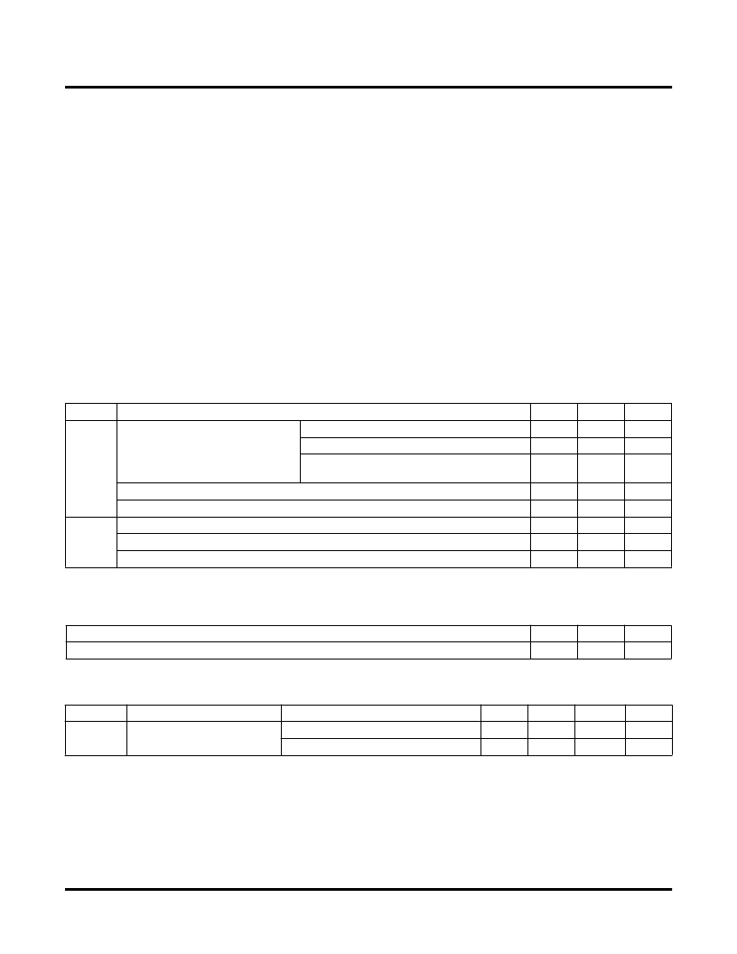
Absolute Maximum Ratings
1, 2, 3
ispMACH 4000C/Z
(1.8V)
ispMACH 4000B
(2.5V)
ispMACH 4000V
(3.3V)
Supply Voltage (V
CC
) . . . . . . . . . . . . . . . . . . . . . . -0.5 to 2.5V . . . . . . . . . .-0.5 to 5.5V. . . . . . . . . . -0.5 to 5.5V
Output Supply Voltage (V
CCO
) . . . . . . . . . . . . . . . -0.5 to 4.5V . . . . . . . . . .-0.5 to 4.5V. . . . . . . . . . -0.5 to 4.5V
Input or I/O Tristate Voltage Applied
4, 5
. . . . . . . . . -0.5 to 5.5V . . . . . . . . . .-0.5 to 5.5V. . . . . . . . . . -0.5 to 5.5V
Storage Temperature . . . . . . . . . . . . . . . . . . . . . .-65 to 150
°
C. . . . . . . . . -65 to 150
°
C. . . . . . . . . .-65 to 150
°
C
Junction Temperature (T
j
) with Power Applied . . .-55 to 150
°
C. . . . . . . . . -55 to 150
°
C. . . . . . . . . .-55 to 150
°
C
1. Stress above those listed under the “Absolute Maximum Ratings” may cause permanent damage to the device. Functional
operation of the device at these or any other conditions above those indicated in the operational sections of this speci
fi
cation
is not implied.
2. Compliance with Lattice
Thermal Management
document is required.
3. All voltages referenced to GND.
4. Undershoot of -2V and overshoot of (V
IH
(MAX) + 2V), up to a total pin voltage of 6.0V, is permitted for a duration of < 20ns.
5. Maximum of 64 I/Os per device with VIN > 3.6V is allowed.
Recommended Operating Conditions
Erase Reprogram Speci
fi
cations
Hot Socketing Characteristics
1,2,3
Symbol
Parameter
Min.
Max.
Units
V
CC
Supply Voltage for 1.8V Devices
ispMACH 4000C
1.65
1.95
V
ispMACH 4000Z
1.7
1.6
1, 2
1.9
V
ispMACH 4000Z, Extended Functional Voltage
Operation
1.9
V
Supply Voltage for 2.5V Devices
2.3
2.7
V
Supply Voltage for 3.3V Devices
3.0
3.6
V
T
j
Junction Temperature (Commercial)
0
90
C
Junction Temperature (Industrial)
-40
105
C
Junction Temperature (Automotive)
-40
130
C
1. Devices operating at 1.6V can expect performance degradation up to 35%.
2. Applicable for devices with 2004 datecodes and later. Contact factory for ordering instructions.
Parameter
Min.
Max.
Units
Erase/Reprogram Cycle
1,000
—
Cycles
Note: Valid over commercial temperature range.
Symbol
Parameter
Condition
Min.
Typ.
Max.
Units
I
DK
Input or I/O Leakage Current
0
≤
V
IN
≤
3.0V, Tj = 105°C
0
≤
V
IN
≤
3.0V, Tj = 130°C
—
±30
±150
μA
—
±30
±200
μA
1. Insensitive to sequence of V
CC
or V
CCO.
However, assumes monotonic rise/fall rates for V
CC
and V
CCO,
provided (V
IN
- V
CCO
)
≤
3.6V.
2. 0 < V
CC
< V
CC
(MAX), 0 < V
CCO
< V
CCO
(MAX).
3. I
DK
is additive to I
PU
, I
PD
or I
BH
. Device defaults to pull-up until fuse circuitry is active.
相關(guān)PDF資料 |
PDF描述 |
|---|---|
| LC4000C | 3.3V/2.5V/1.8V In-System Programmable SuperFAST High density PDLs |
| LC4000V | 3.3V/2.5V/1.8V In-System Programmable SuperFAST High density PDLs |
| LC4000Z | 3.3V/2.5V/1.8V In-System Programmable SuperFAST High density PDLs |
| LC4512x | 3.3V/2.5V/1.8V In-System Programmable SuperFAST High density PDLs |
| LC4512Z | 3.3V/2.5V/1.8V In-System Programmable SuperFAST High density PDLs |
相關(guān)代理商/技術(shù)參數(shù) |
參數(shù)描述 |
|---|---|
| LC4000C | 制造商:LATTICE 制造商全稱:Lattice Semiconductor 功能描述:3.3V/2.5V/1.8V In-System Programmable SuperFAST High density PDLs |
| LC4000V | 制造商:LATTICE 制造商全稱:Lattice Semiconductor 功能描述:3.3V/2.5V/1.8V In-System Programmable SuperFAST High density PDLs |
| LC4000Z | 制造商:LATTICE 制造商全稱:Lattice Semiconductor 功能描述:3.3V/2.5V/1.8V In-System Programmable SuperFAST High density PDLs |
| LC4001B | 制造商:未知廠家 制造商全稱:未知廠家 功能描述:Logic IC |
| LC4001BM | 制造商:未知廠家 制造商全稱:未知廠家 功能描述:Logic IC |
發(fā)布緊急采購,3分鐘左右您將得到回復(fù)。