- 您現(xiàn)在的位置:買賣IC網(wǎng) > PDF目錄383236 > L634 (意法半導(dǎo)體) THREE PHASE MOTOR DRIVER PDF資料下載
參數(shù)資料
| 型號(hào): | L634 |
| 廠商: | 意法半導(dǎo)體 |
| 英文描述: | THREE PHASE MOTOR DRIVER |
| 中文描述: | 三相電機(jī)驅(qū)動(dòng) |
| 文件頁數(shù): | 4/10頁 |
| 文件大?。?/td> | 467K |
| 代理商: | L634 |
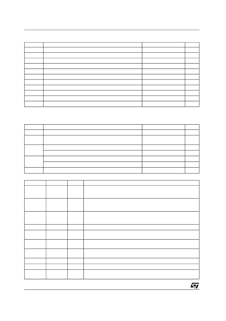
ABSOLUTE MAXIMUM RATINGS
Symbol
V
S
V
IN
,V
EN
I
peak
V
SENSE
V
b
V
OD
f
C
V
REF
P
tot
P
tot
T
stg
, T
j
Parameter
Value
52
– 0.3 to 7
5
-1 to 4
62
60
50
12
2.3
1.6 (*)
-40 to 150
Unit
V
V
A
V
V
V
KHz
V
W
W
°
C
Power Supply Voltage
Input Enable Voltage
Pulsed Output Current (note 1)
Sensing Voltage (DC Voltage)
Bootstrap Peak Voltage
Differential Output Voltage (between any of the 3 OUT pins)
Commutation Frequency
Reference Voltage
Total Power Dissipation
L6234PD
T
amb
= 70
°
C
Total Power Dissipation
L6234
T
amb
= 70
°
C
Storage and Junction Temperature Range
Note 1: Pulse width limited only by junction temperature and the transient thermal impedance
(*) Mounted on board with minimized copper area
RECOMMENDED OPERATING CONDITIONS
Symbol
V
S
V
OD
Parameter
Value
7 to 42
Unit
V
Supply Voltage
Peak to Peak Differential Voltage (between any of the 3 OUT
pins)
52
V
I
out
DC Output Current Power SO20 (T
amb
= 25°C)
4
A
DC Output Current Power DIP (T
amb
= 25°C) with infinite heatsink
2.8
A
V
SENSE
Sensing Voltage (pulsed t
w
< 300nsec)
-4 to 4
V
Sensing Voltage (DC)
-1 to 1
V
T
j
Junction Temperature Range
-40 to 125
°
C
PIN FUNCTIONS
Powerdip
1
20
10
PowerSO20
6
5
15
Name
OUT 1
OUT 2
OUT 3
Function
Output of the channels 1/2/3.
2
19
9
7
4
14
IN 1
IN 2
IN 3
Logic input of channels 1/2/3. A logic HIGH level (when the corresponding
EN pin is HIGH) switches ON the upper DMOS Power Transistor, while a
logic LOW switches ON the corresponding low side DMOS Power.
3
18
8
8
3
13
EN 1
EN 2
EN 3
Enable of the channels 1/2/3. A logic LOW level on this pin switches off both
power DMOS of the related channel.
4,7
9, 12
V
s
Power Supply Voltage.
14
19
SENSE2
A resistance Rsense connected to this pin provides feedback for motor
current control for the bridge 3.
17
2
SENSE1
A resistance Rsense connected to this pin provides feedback for motor
current control for the bridges 1 and 2.
11
16
V
ref
Internal Voltage Reference. A capacitor connected from this pin to GND
increases the stability of the Power DMOS drive circuit.
12
17
V
cp
V
BOOT
GND
Bootstrap Oscillator. Oscillator output for the external charge pump.
13
18
Overvoltage input to drive the upper DMOS
5,6
15,16
1,10
11,20
Common Ground Terminal. In Powerdip and SO packages these pins are
used to dissipate the heat forward the PCB.
L6234
4/10
相關(guān)PDF資料 |
PDF描述 |
|---|---|
| L6353 | Smart Driver for Power MOS & IGBT(用于MOS和絕緣柵雙極晶體管的智能驅(qū)動(dòng)器) |
| L6370 | 2.5A HIGH-SIDE DRIVER INDUSTRIAL INTELLIGENT POWER SWITCH |
| L6370D | 2.5A HIGH-SIDE DRIVER INDUSTRIAL INTELLIGENT POWER SWITCH |
| L6370L | 2.5A HIGH-SIDE DRIVER INDUSTRIAL INTELLIGENT POWER SWITCH |
| L6374 | INDUSTRIAL QUAD LINE DRIVER |
相關(guān)代理商/技術(shù)參數(shù) |
參數(shù)描述 |
|---|---|
| L634F | 制造商:CRYDOM 制造商全稱:Crydom Inc., 功能描述:Power Modules |
| L63500A0GC-30 | 制造商:未知廠家 制造商全稱:未知廠家 功能描述:MIL-STD-1553/ARINC Bus Controller/RTU |
| L63500A0GM-30 | 制造商:未知廠家 制造商全稱:未知廠家 功能描述:MIL-STD-1553/ARINC Bus Controller/RTU |
| L63500A0LC-30 | 制造商:未知廠家 制造商全稱:未知廠家 功能描述:MIL-STD-1553/ARINC Bus Controller/RTU |
| L63500A0LM-30 | 制造商:未知廠家 制造商全稱:未知廠家 功能描述:MIL-STD-1553/ARINC Bus Controller/RTU |
發(fā)布緊急采購,3分鐘左右您將得到回復(fù)。