- 您現(xiàn)在的位置:買賣IC網(wǎng) > PDF目錄374354 > KM4212IM8TR3 (FAIRCHILD SEMICONDUCTOR CORP) Dual, 70A, Low Cost, +2.7V & +5V, 7.3MHz Rail-to-Rail Amp PDF資料下載
參數(shù)資料
| 型號(hào): | KM4212IM8TR3 |
| 廠商: | FAIRCHILD SEMICONDUCTOR CORP |
| 元件分類: | 運(yùn)動(dòng)控制電子 |
| 英文描述: | Dual, 70A, Low Cost, +2.7V & +5V, 7.3MHz Rail-to-Rail Amp |
| 中文描述: | DUAL OP-AMP, 5000 uV OFFSET-MAX, 4 MHz BAND WIDTH, PDSO8 |
| 封裝: | MSOP-8 |
| 文件頁(yè)數(shù): | 6/10頁(yè) |
| 文件大小: | 181K |
| 代理商: | KM4212IM8TR3 |
General Description
The KM4212 is a single supply, general purpose, voltage-
feedback amplifier fabricated on a complementary
bipolar process. The KM4212 offers 7.3MHz unity gain
bandwidth, 9V/
μ
s slew rate, and only 70
μ
A supply
current. It features a rail-to-rail output stage and is
unity gain stable.
The design utilizes a patent pending topology that
provides increased slew rate performance. The common
mode input range extends to 300mV below ground
and to 1.2V below Vs. Exceeding these values will not
cause phase reversal. However, if the input voltage
exceeds the rails by more than 0.5V, the input ESD
devices will begin to conduct. The output will stay at
the rail during this overdrive condition.
The design uses a Darlington output stage. The out-
put stage is short circuit protected and offers
“
soft
”
saturation protection that improves recovery time.
The typical circuit schematic is shown in Figure 1.
Figure 1: Typical Configuration
Power Dissipation
The maximum internal power dissipation allowed is
directly related to the maximum junction temperature.
If the maximum junction temperature exceeds 150
°
C,
some reliability degradation will occur. If the maximum
junction temperature exceeds 175
°
C for an extended
time, device failure may occur.
The KM4212 is short circuit protected. However, this
may not guarantee that the maximum junction
temperature (+150
°
C) is not exceeded under all
conditions. Follow the maximum power derating
curves shown in Figure 2 to ensure proper operation.
Figure 2: Power Derating Curves
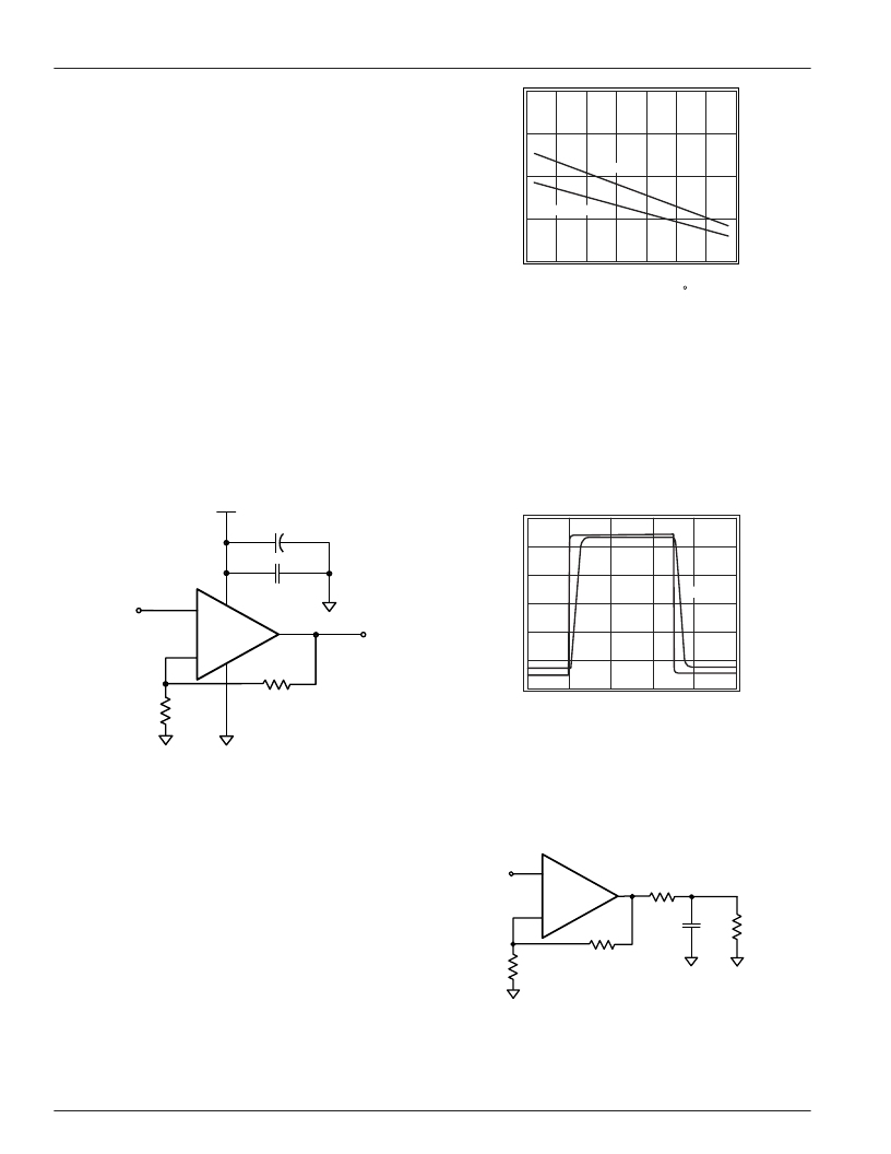
Overdrive Recovery
For an amplifier, an overdrive condition occurs when
the output and/or input ranges are exceeded. The
recovery time varies based on whether the input or
output is overdriven and by how much the ranges are
exceeded. The KM4212 will typically recover in less
than 60ns from an overdrive condition. Figure 3
shows the KM4212 in an overdriven condition.
Figure 3: Overdrive Recovery
Driving Capacitive Loads
A small series resistance (R
s
) at the output of the
amplifier, illustrated in Figure 4, will improve stability
and settling performance.
Figure 4: Typical Topology for driving
a capacitive load
+
1/2
KM4212
-
R
f
0.01
μ
F
6.8
μ
F
+
Out1
+In1
+V
s
R
g
M
Ambient Temperature ( C)
-50
-30
-10
10
30
50
70
90
0
0.5
1.0
1.5
2.0
SOIC-8 lead
MSOP-8 lead
O
I
Time (2
μ
s/div)
Input
G = 5
Output
+
-
R
f
R
g
R
s
C
L
R
L
DATA SHEET
KM4212
6
REV. 1 August 2001
相關(guān)PDF資料 |
PDF描述 |
|---|---|
| KM4212 | Dual, 70A, Low Cost, +2.7V & +5V, 7.3MHz Rail-to-Rail Amp |
| KM4212IM8 | Dual, 70A, Low Cost, +2.7V & +5V, 7.3MHz Rail-to-Rail Amp |
| KM4216C256 | 256K X 16 BIT CMOS VIDEO RAM |
| KM4216V256 | 256K X 16 BIT CMOS VIDEO RAM |
| KM4216C258 | 256K x 16 Bit CMOS Video RAM(256K x 16 位 CMOS視頻RAM) |
相關(guān)代理商/技術(shù)參數(shù) |
參數(shù)描述 |
|---|---|
| KM4-21-30PN | 制造商:Amphenol Corporation 功能描述:KM AUSTRALIAN PRODUCT - Bulk |
| KM4-21-30PN-MK2 | 制造商:Amphenol Corporation 功能描述:KM AUSTRALIAN PRODUCT - Bulk |
| KM4-21-30SN | 制造商:Amphenol Corporation 功能描述:KM AUSTRALIAN PRODUCT - Bulk |
| KM4-21-30SN-MK2 | 制造商:Amphenol Corporation 功能描述:KM AUSTRALIAN PRODUCT - Bulk |
| KM4-21-54PN | 制造商:Amphenol Corporation 功能描述:KM AUSTRALIAN PRODUCT - Bulk |
發(fā)布緊急采購(gòu),3分鐘左右您將得到回復(fù)。