- 您現(xiàn)在的位置:買賣IC網(wǎng) > PDF目錄296260 > K9E2G08U0M-YIB00 256M X 8 FLASH 2.7V PROM, 30 ns, PDSO48 PDF資料下載
參數(shù)資料
| 型號: | K9E2G08U0M-YIB00 |
| 元件分類: | PROM |
| 英文描述: | 256M X 8 FLASH 2.7V PROM, 30 ns, PDSO48 |
| 封裝: | 12 X 20 MM, 0.50 MM PITCH, PLASTIC, TSOP1-48 |
| 文件頁數(shù): | 29/38頁 |
| 文件大小: | 888K |
| 代理商: | K9E2G08U0M-YIB00 |
第1頁第2頁第3頁第4頁第5頁第6頁第7頁第8頁第9頁第10頁第11頁第12頁第13頁第14頁第15頁第16頁第17頁第18頁第19頁第20頁第21頁第22頁第23頁第24頁第25頁第26頁第27頁第28頁當(dāng)前第29頁第30頁第31頁第32頁第33頁第34頁第35頁第36頁第37頁第38頁
FLASH MEMORY
35
K9E2G08U0M
Preliminary
READ STATUS
The device contains a Status Register which may be read to find out whether program or erase operation is completed, and whether
the program or erase operation is completed successfully. After writing 70h command to the command register, a read cycle outputs
the content of the Status Register to the I/O pins on the falling edge of CE or RE, whichever occurs last. This two line control allows
the system to poll the progress of each device in multiple memory connections even when R/B pins are common-wired. RE or CE
does not need to be toggled for updated status. Refer to table 4 for specific Status Register definitions. The command register
remains in Status Read mode until further commands are issued to it. Therefore, if the status register is read during a random read
cycle, a read command(00h or 50h) should be given before sequential page read cycle.
For Read Status of Multi Plane Program/Erase, the Read Multi-Plane Status command(71h) should be used to find out whether
multi-plane program or erase operation is completed, and whether the program or erase operation is completed successfully. The
pass/fail status data must be checked only in the Ready condition after the completion of Multi-Plane program or erase operation.
Table4. Read Staus Register Definition
NOTE :
1. I/O 0 describes combined Pass/Fail condition for all planes. If any of the selected multiple pages/blocks fails in Program/
Erase operation, it sets "Fail" flag.
2. The pass/fail status applies only to the corresponding plane.
I/O No.
Status
Definition by 70h Command
Definition by 71h Command
I/O 0
Total Pass/Fail
Pass : "0"
Fail : "1"
Pass : "0"(1)
Fail : "1"
I/O 1
Plane 0 Pass/Fail
Must be don’t -cared
Pass : "0"(2)
Fail : "1"
I/O 2
Plane 1 Pass/Fail
Must be don’t -cared
Pass : "0"(2)
Fail : "1"
I/O 3
Plane 2 Pass/Fail
Must be don’t -cared
Pass : "0"(2)
Fail : "1"
I/O 4
Plane 3 Pass/Fail
Must be don’t -cared
Pass : "0"(2)
Fail : "1"
I/O 5
Reserved
Must be don’t -cared
Must be don’t-cared
I/O 6
Device Operation
Busy : "0"
Ready : "1"
Busy : "0"
Ready : "1"
I/O 7
Write Protect
Protected : "0"
Not Protected : "1"
Protected : "0"
Not Protected : "1"
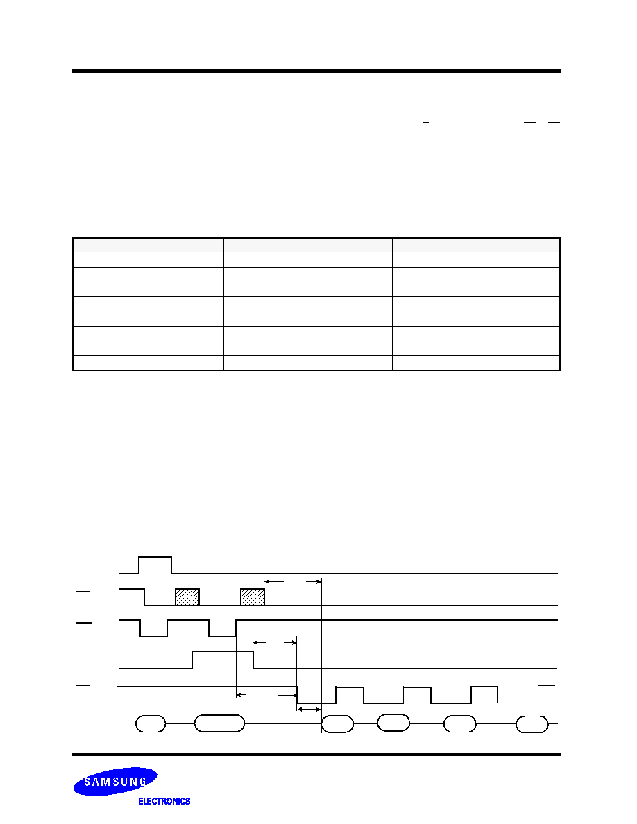
Read ID
The device has 2 types of Read ID command, i.e. Read ID (1) command 90h and Read ID (2) command 91h.
The device contains a product identification mode, initiated by writing 90h to the command register, followed by an address input of
00h. Four read cycles sequentially output the manufacture code(ECh), and the device code (79h), Reserved(A5h), Multi plane oper-
ation code(C0h) respectively. A5h must be don’t-cared. C0h means that device supports Multi Plane operation. The command regis-
ter remains in Read ID mode until further commands are issued to it.
Read ID (2) command 91h provides Multi-Plane(4-Plane) operations availability. If ID code read out by 91h is 20h, it indicates the
device has Multi-Plane(4-Plane) operations.
Figure 21-1 & 21-2 show the operation sequence.
Figure 21-1. Read ID (1) Operation
CE
CLE
I/O0~7
ALE
RE
WE
90h
00h
ECh
Address. 1cycle
Maker code
Device code
tCEA
tAR
tREA
A5h
C0h
Multi-Plane code
tWHR
71h
相關(guān)PDF資料 |
PDF描述 |
|---|---|
| KA-59-281 | TNC CONNECTOR, PLUG |
| KA-91-02 | RF STRAIGHT ADAPTER |
| KA-91-16 | RF TEE ADAPTER |
| KA-99-24 | RF STRAIGHT ADAPTER |
| KA10R25 | 250 A, SILICON SURGE PROTECTOR |
相關(guān)代理商/技術(shù)參數(shù) |
參數(shù)描述 |
|---|---|
| K9F1208B0B | 制造商:SAMSUNG 制造商全稱:Samsung semiconductor 功能描述:FLASH MEMORY |
| K9F1208B0C | 制造商:SAMSUNG 制造商全稱:Samsung semiconductor 功能描述:64M x 8 Bits NAND Flash Memory |
| K9F1208B0C-P | 制造商:SAMSUNG 制造商全稱:Samsung semiconductor 功能描述:FLASH MEMORY |
| K9F1208D0A | 制造商:SAMSUNG 制造商全稱:Samsung semiconductor 功能描述:64M x 8 Bit , 32M x 16 Bit NAND Flash Memory |
| K9F1208D0A-P | 制造商:SAMSUNG 制造商全稱:Samsung semiconductor 功能描述:64M x 8 Bit , 32M x 16 Bit NAND Flash Memory |
發(fā)布緊急采購,3分鐘左右您將得到回復(fù)。